Siemens Industrial Edge and FFT DataBridge connect shopfloor and plant data directly to the Databricks Platform – no IoT middleware required New edge to cloud connectivity offers scalable advanced analytics and a unified, AI‑ready production data foundation Industrial customers can optimize their operations, reduce costs and increase productivity Siemens announced...
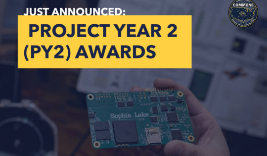
The Microelectronics Commons NSTXL (National Security Technology Accelerator) has announced the DoW Year 2 awards, with more than $200M invested across 26 projects nationwide and the Southwest Advanced Prototyping (SWAP) Hub earning continued support for multiple high-impact efforts already advancing U.S. microelectronics innovation. These awards recognize real progress and growing...
A patient who can no longer speak generates text directly from neural activity. A patient with paralysis controls a cursor using thought alone. Behind demonstrations like these is a difficult engineering problem: how do you assemble electronics delicate enough to interact with the human brain, while keeping them stable inside...
By Thomas McMahon Naval Surface Warfare Center, Port Hueneme Division, CA Sailors can now get certified in operating and maintaining the fleet’s most prevalent directed energy system through a new training program at Naval Surface Warfare Center, Port Hueneme Division (NSWC PHD)’s Directed Energy Systems Integration Laboratory (DESIL), with the first...
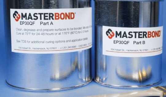
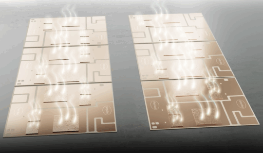
Understanding common failure mechanisms allows engineers to implement preventive measures during the design and qualification phases. Delamination and Bond Failure...
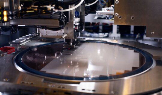
Wafer cleaning is one of the most critical steps in the semiconductor process flow, especially as dimensions continue to shrink to below the 1-nanometer (nm) node. Photoresist residue and particulates can...
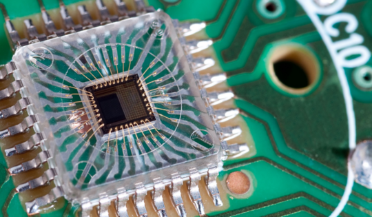
Introduction On average, cars today contain 1,700 semiconductor chips, underscoring how crucial they are to automobiles. Semiconductor chips support a...
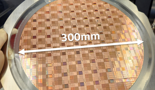
AI is transforming the next-generation advanced foundry for 2nm chips, thus reshaping the semiconductor industry, writes Rozalia Beica. The semiconductor...
Overview of MasterSil 153 Master Bond MasterSil 153 is a two-component paste silicone compound for high-performance bonding and sealing applications....
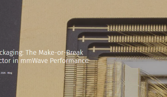
Millimeter-wave (mmWave) technology occupies the short-range, high-frequency portion of the electromagnetic spectrum—typically defined as 30 to 300 GHz—and is enabling...
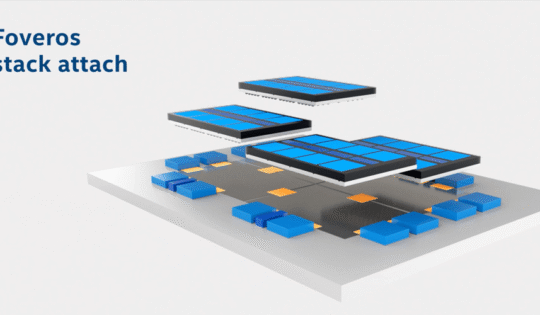
The semiconductor industry finds itself at a critical juncture, where the traditional paradigms of Moore’s Law are encountering fundamental physical...