Every metal layer on a wafer, from M1 at the front end to redistribution for wafer-level packaging (WLP), requires patterning. Selective material removal, including etching oxides and metals, often becomes the critical path. It is essential to thoroughly strip photoresist and minimize contamination to achieve the desired yield. Plasma etching enables successful results.
The finer the features and the greater the number of layers, the more necessary it is to achieve precise, repeatable patterns during lithography. Vertical architectures like 3D NAND with many layers and high aspect ratios (HAR) step up the processing challenge. The structures need vertical sidewalls and contamination-free surfaces. The process window is extremely narrow. Every deposition and etching step must be optimized, or yield will suffer.
Two general approaches for removing material from a wafer surface are wet chemical etchants and dry plasma etching. Choices between the two technologies depend on multiple factors, and fabs will often use wet and dry processing together, selecting the best option for each process step or product type. There are often tradeoffs between speed and selectivity that need to be considered to achieve the best result.
Plasma etching is used in several different process steps. These include:
- Etching of oxide, nitride, metal, and polyimide layers
- Ashing to strip the photoresist after patterning metal and oxide layers
- Descumming to remove any photoresist remaining after patterning each layer
This article discusses plasma etching technology, focusing on reasons to choose plasma over wet etching. It comes down to three things: process flexibility, consistency, and traceability.
Tailoring plasma etching
Plasma etching is precise, flexible, and compatible with many different processes. Depending on the gas used to create the plasma, it can remove metals or dielectrics from various substrate materials.
Adjusting the gas composition, pressure, flow rate, and temperature affects the etch rate and selectivity. Precise tailoring of the plasma chemistry allows plasma etching to be highly selective, removing the target material while leaving other areas of the wafer untouched. In practice, it can take extensive modeling and testing to develop a recipe that will achieve the necessary selectivity and not damage previously deposited layers.
Plasma can be made from a wide range of gasses, including oxygen, hydrogen, nitrogen, helium, methane, and more. Ashing, for example, uses oxygen plasma at a temperature of around 250 °C to burn off the photoresist. The descum process is much gentler and runs at a lower temperature.
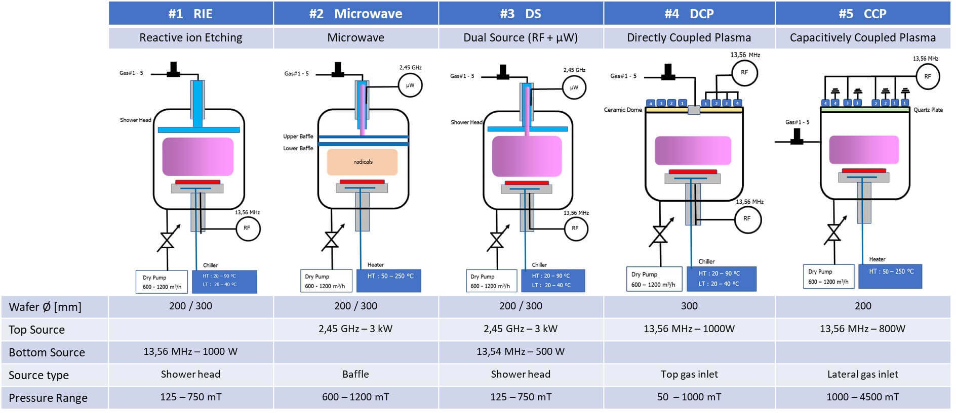
The power source generating the electricity needed to ionize the gas to form plasma can be radio frequency (RF), microwave, or a combination of the two. Multiple reactor types (Figure 1) allow for greater flexibility in processing conditions. Facilities can select the option that best meets their temperature and pressure requirements, and choose equipment that fits into their process flow and available footprint.
Other options include capacitively coupled or inductively coupled plasma. Capacitively coupled plasma has typically been used for etching dielectrics, while high-power inductively coupled plasma is more commonly used for etching metals (Figure 1).
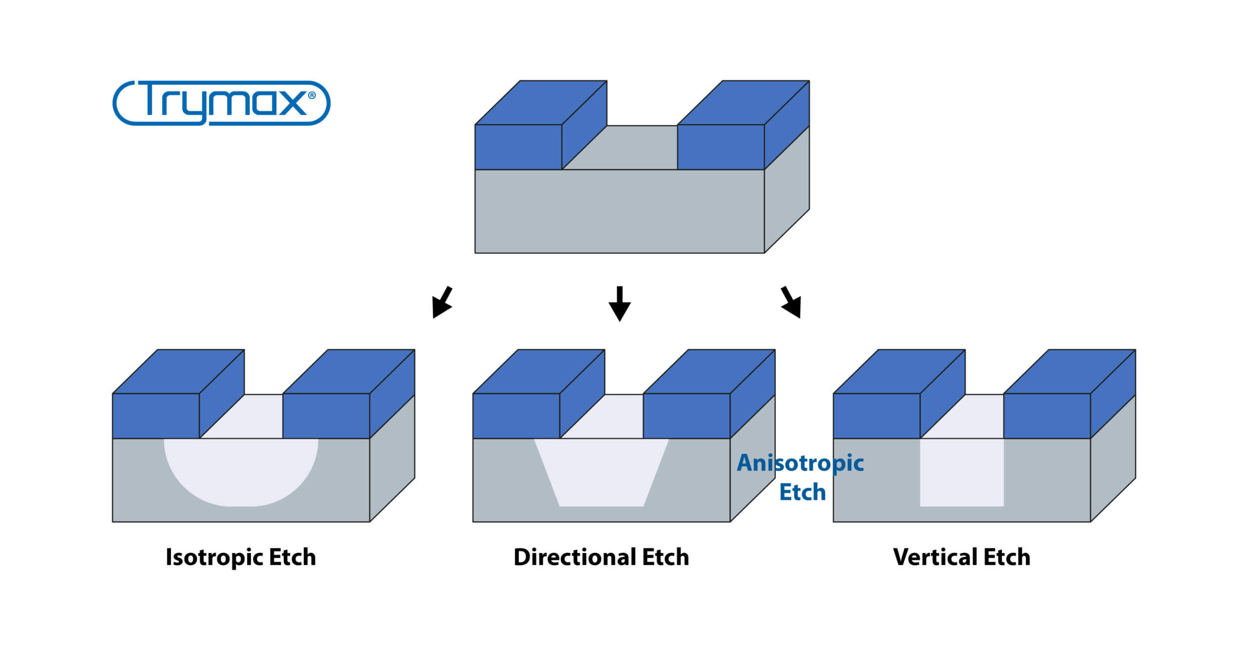
Plasma offers excellent etch control, including controlling whether material removal is isotropic (the same in every direction) or anisotropic (faster removal on one part of the surface), as shown in Figure 2. This flexibility is especially beneficial for removing layers from trenches in HAR structures. Controlled anisotropic etching minimizes the risk of over-etching the bottom of the trench to achieve sufficient material removal from the sides.
Consistent Results
Consistent results from wafer to wafer are necessary to maintain high, repeatable yield. Consistency is another aspect where wet and dry etch differ.

Wet etch immerses an entire cassette of wafers at once. Each batch that goes through the process affects the bath chemistry. The first wafers that go through after a bath change will experience pristine, ideal conditions. By the time later batches go through, contamination or chemical degradation can cause the yield to drop. More frequent bath changes can mitigate this effect, but that increases chemical consumption and waste.
Plasma chambers usually process one wafer at a time under conditions that remain stable. Once input parameters are set, the gas flow rate and pressure are always the same. Continual monitoring will flag any deviations and pause processing. The substrate temperature is also monitored and controlled. Because plasma process conditions can be tailored to the materials and requirements for each application, and wafers are processed one at a time, consistency is easier to achieve.
Better Traceability
One-by-one processing also improves process control and traceability. The process will stop if data shows that a measurement is out of specification. A technician will make the necessary adjustments and restart the equipment. At most, one wafer will be affected versus an entire cassette.
If inspection further down the line shows repeating defects, data on every wafer that went through the plasma chamber is available. Analyzing this data can indicate whether anything in the plasma process was responsible for the yield loss, improving traceability and failure analysis. This option is not available with batch processing.
Automotive and biomedical markets are especially sensitive to the need for repeatably producing reliable devices, as human safety is in play. They want to see comprehensive failure analysis and appreciate track and trace capabilities at the wafer and chip level.
Conclusion: The Need for Plasma is Growing
While wet etch is not going away, and some products and process steps are well-suited to wet etch, we believe that plasma use will continue to accelerate. At advanced nodes, some geometries cannot be patterned with wet etch. Power integrated circuits (ICs) for automotive and 5G applications are often built on silicon carbide (SiC) or gallium nitride (GaN) substrates for greater efficiency in high-voltage, high-frequency operating environments. Standard wet etchants do not work on these materials. This is a growing market where the flexibility of plasma etch can meet the requirements.
Another reason the plasma market is growing is the increasing demand for tracking and tracing at the wafer and chip level. This requirement will expand beyond the automotive and medical industries to more applications.
There is a need for machines that can take full advantage of the flexibility of plasma processing (figure 4). Tools like the Trymax NEO series that can handle a wide range of input gases, switch between sources, handle different substrates, and process multiple wafer sizes are well-positioned to serve the entire semiconductor industry.