Who Is This For This article is for photonics and semiconductor engineers, optical-module designers, reliability teams, datacenter-network architects, and technical...
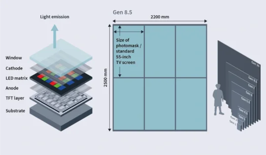
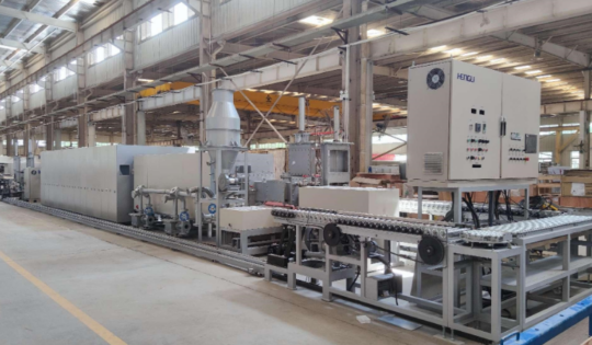
Modern flat-panel displays depend on highly complex multilayer structures fabricated on enormous glass substrates. As display generations continue to grow,...
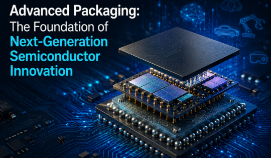
As federal agencies and defense organizations race to modernize the technologies that underpin national security, the semiconductor industry has entered...
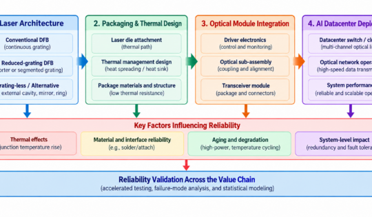
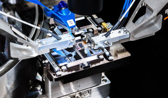
The rapid development of artificial intelligence (AI), high-performance computing (HPC), and hyperscale data centers is creating unprecedented demand for bandwidth...
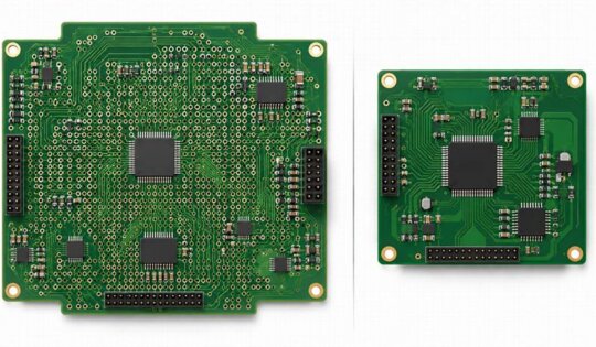
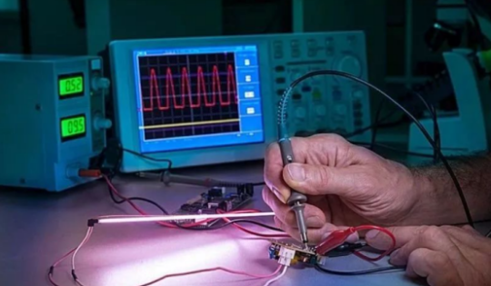
Introduction Even experienced electronics engineers can overlook design decisions that appear minor during development but later result in higher manufacturing...
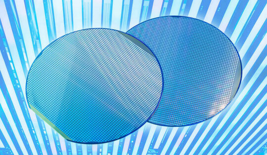
Wafer cleaning is one of the most critical steps in the semiconductor process flow, especially as dimensions continue to shrink to below the 1-nanometer (nm) node. Photoresist residue and particulates can...
Multilayer ceramic capacitors (MLCCs) are widely used electronic components made by stacking many thin ceramic dielectric layers with internal electrodes....
AI is transforming the next-generation advanced foundry for 2nm chips, thus reshaping the semiconductor industry, writes Rozalia Beica. The semiconductor...
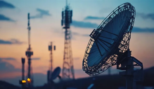
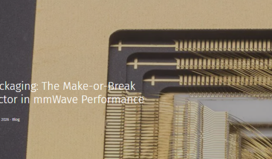
Millimeter-wave (mmWave) technology occupies the short-range, high-frequency portion of the electromagnetic spectrum—typically defined as 30 to 300 GHz—and is enabling...