NanoCleave enables Laser Debonding on Silicon with Nanometer Precision
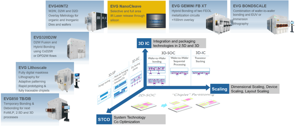
In semiconductor manufacturing, 3D integration – the manufacturing, vertical assembly, and packaging of multiple different dies into a single package – is increasingly important in optimizing the power, performance, area, and cost (PPAC) metric in semiconductor design and manufacturing, as well as enabling roadmap continuation. At the same time, wafer bonding is a critical enabler for 3D integration. One can even argue that wafer bonding is the new lithography scaling because without temporary and permanent wafer bonding one cannot vertically stack components and dies (Figure 1).
In the past, 3D integration was driven primarily from a packaging perspective. In other words, different dies on interposers or fan-out wafers were connected to each other, with considerable performance increases. However, the dies were designed and manufactured as a classically 2D system on a chip. Despite enormous efforts and successes in the area of lithography and transistor node reduction, performance increase has slowed down and requires a rethink in the manufacture and design of future processors and memories. Above all, there is no way around 3D integration and wafer bonding or layer transfer.
Moving Beyond Glass Carriers
Carrier technologies utilizing glass substrates, coupled with organic adhesives and wafer bonding processes, have become an established method for building up device layers in 3D devices. The device wafer is temporarily bonded onto the glass carrier wafer using the organic adhesive, where it is then thinned on the backside. Next, an ultraviolet (UV) wavelength laser is used to dissolve the adhesives and release the device layer, which is subsequently permanently bonded onto the final product wafer.
However, glass substrates are difficult to process with semiconductor fab equipment that has been designed primarily around silicon, and that requires costly upgrades to enable glass wafer processing. Simple things such as wafer edge detection and pre-aligners can be upgraded to make established equipment carrier compatible. More fundamental issues with glass carriers are their electrical and thermal isolation properties, which demand new recipes for deposition or the deposition of extra layers on the wafer backside to allow electrostatic chucking in deposition and etch equipment. In addition, organic adhesives are generally limited to processing temperatures below 300°C, which limits their use in back-end processing.
In a perfect world, fabs could utilize silicon carriers with inorganic release layers to avoid these temperature and glass carrier compatibility issues. Recently, a revolutionary layer transfer approach was introduced that eliminates the need for glass substrates for advanced packaging. This avoids both temperature and glass carrier compatibility issues and enables the ability to transfer ultra-thin (single micron and below) layers via carriers in front-end processing without changing the processes of record.
NanoCleave Infrared Laser Release Technology
This new layer release technology for silicon, called NanoCleave™, utilizes an infrared (IR) laser and specially formulated inorganic release materials to enable laser debonding on silicon with nanometer precision. The backside of the silicon wafer is exposed to the IR laser, which operates at a unique wavelength to which the silicon is transparent. An inorganic release layer that is pre-built into the silicon stack through standard deposition processes absorbs the IR light, resulting in the cleaving of the silicon at a predetermined and precisely defined layer or area.
Utilizing inorganic release layers enables more precise and thinner release layers to be used in the range of a few nanometers versus a few microns for organic adhesives. Subsequent stacking of such thin device layers enables higher bandwidth interconnects, and opens new opportunities to design and segment dies for next-generation high-performance systems. In addition, the inorganic release layers are compatible with high-temperature processing (up to 1000°C), enabling layer transfer for many new front-end applications, such as epitaxy, deposition, and annealing, where organic adhesives are incompatible.
The nanometer-precision of the NanoCleave process supports advanced semiconductor device roadmaps calling for thinner device layers and packages, increased 3D integration, and reduced processing costs through thin-layer transfer and the elimination of glass substrates. At the same time, NanoCleave’s compatibility with high-temperature processes enables hybrid and fusion bonding even of ultra-thin layers on silicon carriers, which in turn enables completely novel process flows for 3D IC and 3D sequential integration applications.
For interposers, several improvements in integration and patterning density are on the industry roadmap for leading-edge applications below 500nm line/space patterning resolution. Furthermore, integrated passive devices require high process temperatures (more than 300°C) for dielectric deposition and etching. This is generally unsuitable for adhesive-based carrier systems since the processing temperatures of most thermoplastic and thermoset materials are limited to 270°C.
For fan-out wafer-level-packaging (FOWLP), glass carriers are now standard and meet many requirements of today’s packages and interconnect densities down to about 2µm linewidths. However, new concepts are needed to take FOWLP further with linewidths well below 1µm. This is very easy to realize with silicon carriers and IR debond and allows seamless copper and dual damascene integration.

Enabling Die-to-Wafer Hybrid Bonding
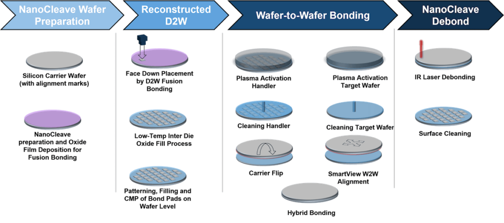
Reconstructed wafers circumvent the restriction of wafer-to-wafer (W2W) bonding by allowing tested good dies to be placed on a carrier substrate and then filling the gap between dies with a dielectric oxide filling process. In this way, a continuous wafer with an oxide surface serves as a base for further process steps. Figure 2 describes the process flow in detail.
One of the main reasons for this process flow is to eliminate traditional packaging materials and replace them with fab-clean and fab-standard materials. This shifts the standard packaging process from back-end-of-line processing to the fab front-end where interconnects are being processed. As a result, more and thinner layers of interconnects in chip processing can be achieved than ever before.
NanoCleave is perfectly suited for enabling silicon as a starting carrier due to the following reasons:
- It provides for a fusion bondable surface to attach chips top side up or bottom side down for mechanical attachment
- It provides the high-temperature capability for all standard fabrication processes at process temperatures of 450°C and higher
- It combines with W2W hybrid bonding to enable layer transfer and uniform stacking of multiple thin wafers, enabling high bandwidth interconnects
- It enables the delamination of ultra-thin films in the sub-micron range
Ultra-thin Layer Transfer and Stacking Using “Temporary” Fusion Bonding
Another significant application of NanoCleave is the combination of IR laser release technology with fusion bonding, which enables fusion bonding to carriers and then area-selective detachment after processing. The IR laser release technology is based on front-end compatible and available materials and deposition processes. This means there are no limitations in process temperature, that the NanoCleave and release of the product wafer can be conducted without any adaptive process, and that integration flows do not need to be adapted and requalified due to new materials in the line. Another key advantage of using inorganic release layers is their high film uniformity in combination with fusion bonding. As the materials are highly uniform over the wafer and do not alter their properties during processing, the NanoCleave carrier system enables a tremendous reduction in device thickness to sub-micron without damage resulting from the carrier process.
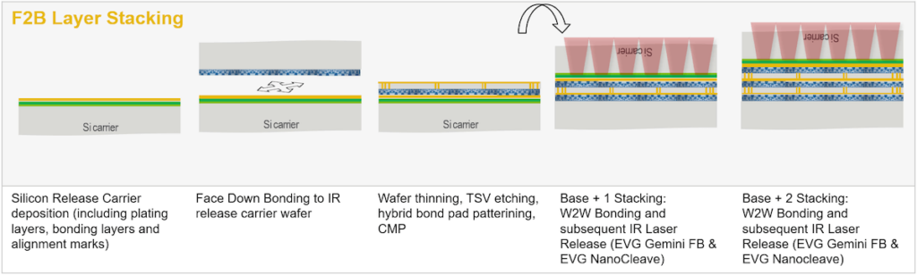
Especially in hybrid bonded memory applications, such as SRAM or DRAM, carrier systems have a crucial role in wafer stacking. To stack the same wafer layouts, without mirroring one of the devices, face-to-back stacking is needed where one device wafer is mounted, thinned, and backside processed on a carrier used for hybrid bonding (Figure 3). By freeing any temperature restrictions and enabling ultra-thin silicon processing, through silicon vias of 50µm depth can become through silicon contacts of only a few microns, resulting in improved thermal, electrical, and better cost performance. As a result, NanoCleave carriers are a key enabler for using hybrid bonding on ultra-thin device wafers.
Conclusion
Wafer bonding and layer transfer are critical enablers of 3D integration. Glass carriers and inorganic adhesives have traditionally been used for building up layers in 3D devices. However, continued roadmap scaling requires a new approach to layer transfer technology. A novel and universal IR release technology through silicon wafers, called NanoCleave, has been developed that provides precisely controlled cleaving without IR transmission or risk to the device layer. The use of inorganic IR release layers enables nanometer-precision separation of layers and higher processing temperatures, thereby supporting front-end processing and enabling die and wafer processing with thicknesses below 1µm for improved PPAC. The NanoCleave technology is demo ready at EV Group’s Heterogeneous Integration Competence Center™ (HICC) – the company’s innovation incubator for heterogeneous device integration – located at its headquarters in Austria.
Beyond today’s application, wafer bonding and NanoCleave can play a key role in upcoming device developments by providing a boost to lithography scaling for 3D sequential and even new transistor designs, such as complementary FET (CFET). Further research into this is being investigated.
Editor’s Note: This article originally appeared in the 2023 Yearbook. Read the full issue.