
Almost four years ago, we published an article titled “CoolCube™: A True 3DVLSI Alternative to Scaling” on 3D InCites. It described the concept of stacking layers of transistors sequentially on top of each other and documented the research effort happening at Leti to develop a feasible process integration scheme and a comprehensive product design frame. Now, four years later, we can say that pioneering this true 3D VLSI concept has put Leti in a very good position to lead the next few decades of innovation in microelectronics.
In reality, the limits of 2D scaling described three years ago remain, and are even more present than before, calling for a new approach that includes 3D capabilities. Fewer than four fab companies are producing 2D technology below 10nm. Cost-of-ownership for those nodes is skyrocketing to such levels where only a few ICs can assure a return on investment. Even if several applications require those bleeding edge technologies, most companies are now looking to enable innovative 3D stacking flows (Figure 1).
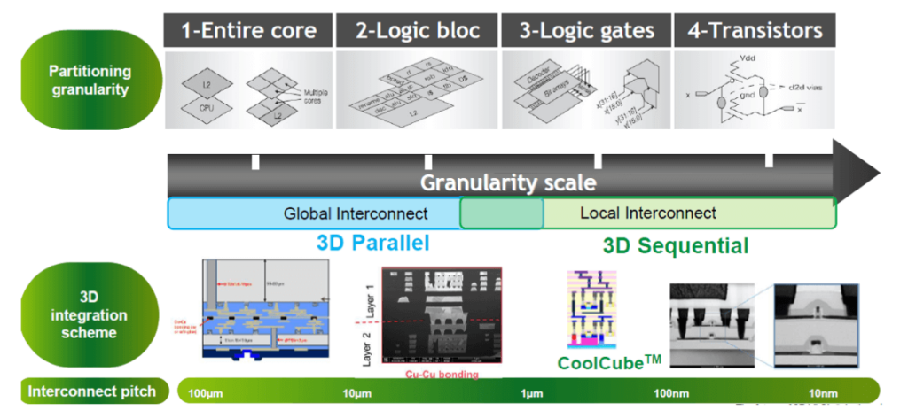
For systems requiring high performance, advanced 3D technologies such as hybrid bonding and monolithic 3D are considered to be the only ways to push computing to higher levels, given desired targets for memory capacity, memory bandwidth, power efficiency, reliability, and cost. For systems requiring heterogeneous applications, those technologies provide multiple opportunities to enable efficient edge computing of sensor data.
Towards 500°C device, and below
3D sequential integration aims to provide a concept for stacking devices with a nanometer scale resolution, allowing low aspect ratio and small 3D‐contact fine‐grain interconnects. It requires limiting the thermal budget of the top tier processing to a low temperature (less than 500°C) in order to ensure the stability of the bottom devices.
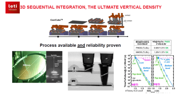
Leti’s 3D sequential integration concept is called CoolCube. After more than ten years of research, Leti is now able to present breakthrough proof points in several areas that were previously considered as potential showstoppers for 3D sequential integration.
Either from a manufacturability, reliability, performance, or cost point of view, on a 300mm FDSOI advanced platform, experimental data from Leti has now demonstrated the ability to obtain:
- Low-resistance poly-Si gate for the top field effect transistors (FETs)
- Full low-temperature raised source and drain (LT RSD) epitaxy including surface preparation
- Stability of intermediate back-end-of-line (BEOL) between tiers with standard ultra-low-k (ULK) copper (Cu) technology
- Stable bonding above ULK
- Efficient contamination containment for wafers with Cu/ULK intermediate BEOL, enabling their re-introduction into the front-end-of-line (FEOL) for top FET processing
- SmartCut™ process above a CMOS wafer
Leti’s work has focused on functionality demonstrations of the CoolCube concept. However, some performance measurements already enable validation of the concept for certain electrical device specifications:
- At 500°C, compared to a high-temperature process scheme, no degradation of bottom MOSFETs has been measured.
- On 2D readout and on 3D full stacking, we demonstrated the capability to form the junctions at low temperature without any performance degradation (Ion, Vt) for the top layer N or P devices. Slight degraded values are not due to mobility but to access resistance, something greatly improved by replacing the nitride spacer.
- For bottom level transistors, we observed no change in terms of reliability. Top level transistors meet lifetime requirements at 5 and 10 years, additional gate stack solutions investigated on short-loop lots are promising to improve the reliability level to be measured on the full-3D CoolCube (Figures 2a and b)
Leti generated a portfolio of almost 50 patents around the CoolCube concept, the first one issued in 2008. However, Leti is no longer the only technology research organization working on 3D sequential integration. NARLAB, located in Taiwan; and imec, in Belgium, are also presenting papers on this subject at major conferences, increasing momentum of the concept for the future of microelectronics.
Cost Figures
Beside process integration research, Leti has also studied the cost figures of 3D sequential integration. If such integration is widely seen as a technological push, the economic benefit is not evident. Most initial reactions towards this concept are to anticipate a clear drawback for digital applications: complexity factors, doubling expensive process modules, doubling lead-time, etc.
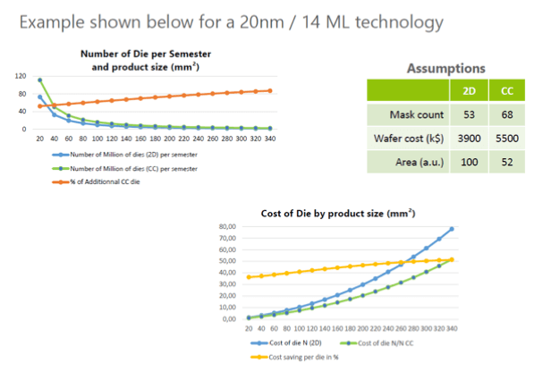
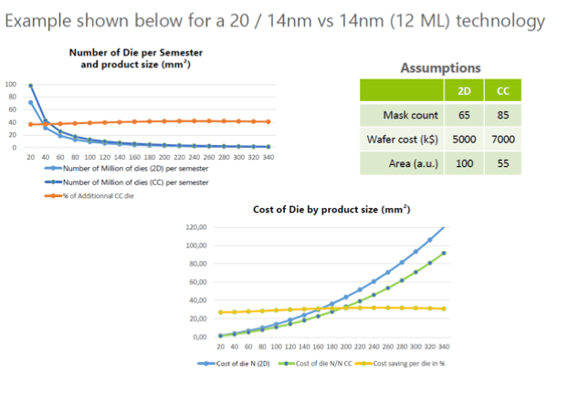
To establish parameters, Leti developed a unique analytical cost model to benchmark any technology node, or 3D integration scheme compared to 2D. Based on die area, yield and mask count, this model considers any benefit of the concept considering also time to market, volume ramp-up, or new functions integration.
A main outcome of the study reveals that smart tiers/blocks/functional partitioning will be key to fully benefit from 3D sequential integration without any design evolution or circuit architecture changes. Re-using 2D standard IP blocks and depending on the applications, there is a need to structure top and bottom tiers following the different block configurations:
- Data IPs (computing path), Memory (SRAM/ROM): High performance but wire congestion
- Clock tree: Keep accuracy and good circuits placement, very sensitive to BEOL loading
- Logic I/O, Analog/RF and passive: Dedicated process options required
- Service functions (as test/power management): Less performance-driven but close imbrication with Data IPs
For evaluation, two main implementations are tested: Node N over Node N and Node N-1 over Node N. Both implementations are compared to a 2D Node N configuration. Although it exhibits additional process complexity with an impact on yield or cycle time, for example, for digital products based on homogeneous stacking of N/N nodes, the model shows that 3D sequential integration provides significant cost savings (Figure 3). These savings are essentially due to the area reduction and the increased number of dies per wafer. From one node N to another, slight variations of the results are obtained but the trend is the same. Reusing validated IP on older than 28nm nodes is compatible with advanced node 3D integration and shows both cost saving and dies supply improvement.
We also recognize that 3D sequential technology is suitable for applications that require heterogeneous functions. Smart partitioning between the two devices layers may reduce process options and save cost. Mixed-signal applications such as a smart sensor, actuator, and interface (visible and IR imaging, nanoelectromechanical systems (NEMS) array, LED…) are particularly interesting; 3D HD interconnects (MIV) and fine-grained partitioning drastically reduces the footprint and save power. 3D sequential technology is also very promising in computing systems. In this case, the partitioning can be done between logic and other hardware IPs such as SRAMs, rapid IOs, signal converters, test infrastructure, and power management.
A complete EDA environment to design 3D test chips on CoolCube technology
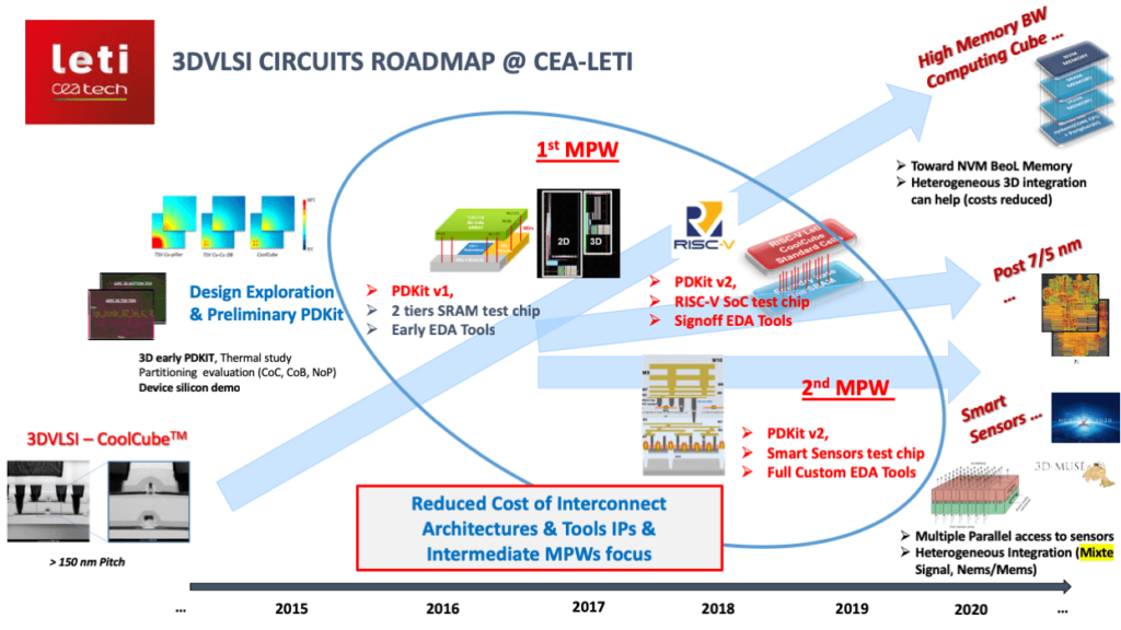
During the last four years at Leti, a 2-layer technological and application design environment has been developed to design and fabricate real circuits as demonstrators of this 3D sequential integration. The recent H2020 3D-Muse project lead by Leti started in January 2018. It will allow us to deliver a first proof of concept.
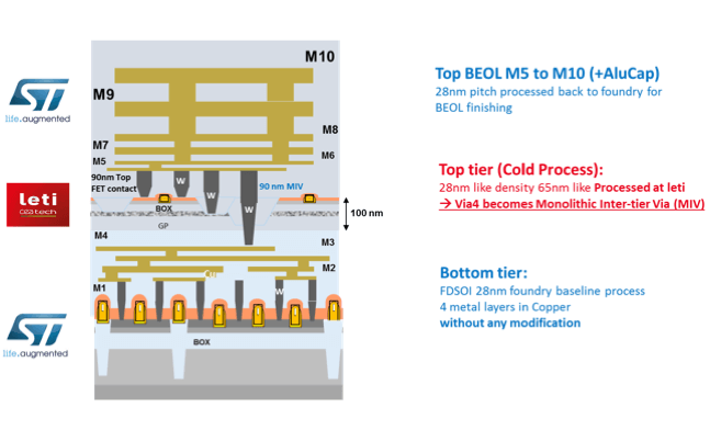
CoolCube devices and MIVs are inserted between the M4 and M5 metal levels in a standard 10ML 28nm FD-SOI process from STMicroelectronics. A unified design environment based on an incremental technology database (ITDB) framework is available to design test chips in a routine multi-project wafer (MPW) at ST Microelectronics’ advanced fab. Both the active layers and the whole metal stack are managed using similar tools and methods already well-known in 2D design: spice models, pcells, design rules check (DRC), layout versus schematic (LVS), parasitic extraction (PEX) of both layers, and global post-layout simulation (PLS) (Figures 4a & b).
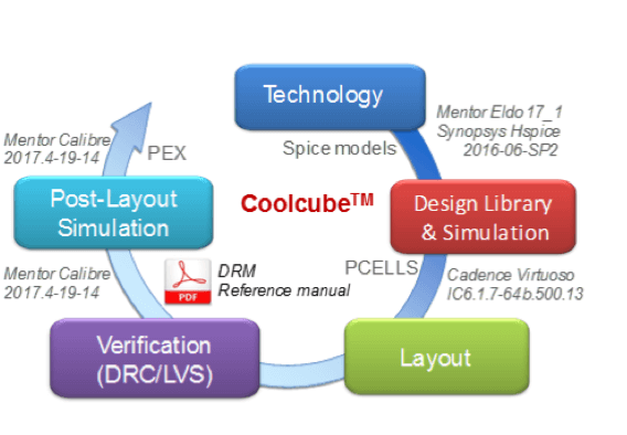
Spice models use data measured acquired on CoolCube process development engineering lots. Both 28nm FD-SOI and CoolCube technology stacks are merged to perform technology computer-aided design (TCAD) simulations and to align top layer RC parameters extracted at the design level using Mentor Graphics Calibre XACT tool.
On the CoolCube layer, a standard-cell-based digital design is available using classical logic synthesis (Synopsys DC-Compiler 1-2016.03) and place and route tools (Cadence Innovus 16.20). In the context of logic on IPs (SRAMs or other) MIVs are managed automatically by the tools (power distribution from thick metal layers to bottom IPs, signal interconnects between bottom IPs and top standard cells). 36 standard cells are today available, allowing a first routine circuit design:

- Inverters: IVX9, IVX18, IVX35, IVX71
- Buffers: BFX9, BFX18, BFX35, BFX71
- Logic gates: NAND2X7, NAND3X5, NOR2X6, NOR3X4, XNOR2X9, XOR2X9, AOI12X6, AOI211X9, AOI22X6, OAI12X6, OAI211X11, OAI22X6
- Flip-flops: SDFPQX9, SDFPRQX9
- Balanced cells: CNIVX10, CNIVX21, CNIVX41, CNIVX62 and latch: CNHLSX10 for gated-clock tree
- Decoupling cells: DECAP8, DECAP16
- Filler cells: FILLERPFP1, FILLERPFP2, FILLERPFP4, FILLERPFP1-CO3D, FILLERPFP2-CO3D, FILLERPFP4-CO3D;
- Well-tap cell: FILLERSNPWP-FP4_GP are available including classical views for P&R, Verilog and spice simulation, ATPG…
- A first set of I/O pads compatible with CoolCube is also available to build an I/O ring and develop any test chip in a package
The common ground plane is used to adjust the threshold voltage after fabrication; specific fillers (FILLERPFPx-CO3) ensure DRC clean design when the ground plane is opened due to the presence of MIVs.
Design flows and methodologies
Since the previous article we published on the subject four years ago, the Leti design team has also worked on a set of methodologies to properly design a circuit using the CoolCube concept. For a PLS and PEX module, a deck of MIPT format files is available that contains the description of the top-level stacking (FEOL/BEOL), bottom level considered as substrate (emulation), and also includes technical information such as metal resistivity, contact resistance, etc. and corner type. The output is a netlist including resistor-capacitor (RC) parasitic elements and standard cell characterization. CoolCube circuit design uses signoff 2D tools, reuses 2D power mesh and clock tree, and co-optimizes cell density from one tier to the other. Digital flow & CAD tools are regular tools such as:
- Synthesis flow using Synopsys DC Compiler with LIB & DB files (function/timing) and cell characterization (based on spice simulation with layout)
- Place and route flow using Cadence Innovus with LEF techno (techno and routing information including MIV rules), QRC tech file (3D stacking definition, RC data generated from ICT file) and LEF files (SC layout abstract view)
A first evaluation has been done to compare thermal performances of different 3D technologies, something that is always put forward when we talk about 3D. To compare TSV+µ-bumps, hybrid bonding, and CoolCube, we use a simple method that defines a representative set of experiments, different technology parameters (number of layers, 3D interconnection pitch, materials, etc.), a different power scenario, and thermal dissipation scheme. The thermal model used is the SAHARA tool from Mentor Graphics. The results show a better thermal coupling for hybrid bonding and CoolCube, a reduced hot-spot effect, but also a strong sensitivity to interconnect density and die thickness.
A second MPW was launched to examine multi-tier embedded memory/multiple arrays on periphery partitioning to look at the advantage of 3D compared to a 2D architecture (Figure 5). The bottom level was dedicated to all decoding logic, drivers, I/Os, and redundancy. The top level was a 128×128 SRAM array connected by MIVs. Three scribe lines have been designed, including a 2D reference 16kb SRAM with 32-word redundancy blocks, and two 3D 16kb SRAM with 32-word redundancy block either using MIVs or single 3D TSVs. The objective will be a first tape out at IP level (building block) but early results from layout show a 40% footprint reduction, with ~100000 transistors on top cold process, and 2068 MIVs – Density: 37600 MIVs / mm². Based on the same methodologies, a second test chip resolving a 32-bit RISCV (RI5CY) SoC will be embedded in the 3D Muse MPW in order to perform a real case benchmark between 3D and 2D.
Test cases, applications, and future work
After more than ten years of research and development, Leti sees the CoolCube concept becoming a common platform for multi-application-driven technological developments. Leti’s strength has been to gather a full ecosystem of partners around its program, including materials companies, tool suppliers, EDA providers, fabless and fab companies, test, and characterization support. Leti is now implementing the first application engagements in industrial product roadmaps to get the full benefit of the technology.
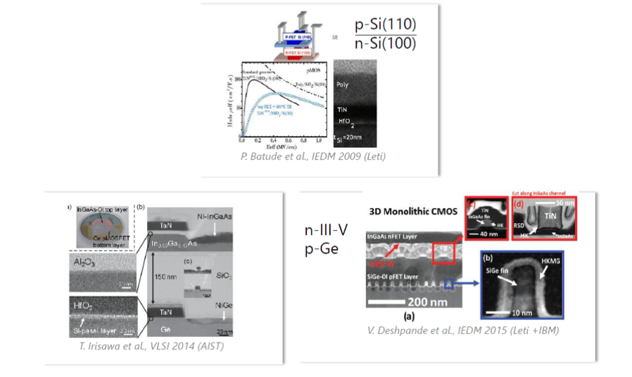
A first application of the concept will be to enable partitioning up to the transistor device scale (Figure 6). When imaging N/P or P/N FET stacking, an enormous gain is obtained by boosting each FET performance independently on each level. Each FET polarity would pick up the best possible channel material, gate stack, stressors or contact metallurgy. A 3D fine connection at the device level will provide device-level outperformance (current/capacitance) and will spare front-end players numerous expensive lithography steps and process selectivity challenges vs. planar 2D schemes. This Holy Grail nevertheless requires a redesign of all libraries and standard cells with a limited area gain, much below 50%, considerably reducing the area gain for SRAM, for example.
Leti is also relying on a CMOS over CMOS approach as we have seen earlier. The first ideas are coming for new digital architectures including logic-on-memory for data-intensive computing (data analytics or data retrieval), and of course for neuromorphic convolutional neural networks for deep learning and artificial intelligence accelerators. Both test cases are dominated by memory and wires, organized as a parallel matrix of computational data loading, with performance obviously enhanced by the density of contacts allowed by the CoolCube integration. It really can be seen as an extension of 3D hybrid bonding for close memory/logic entanglement and disruptive design approaches.
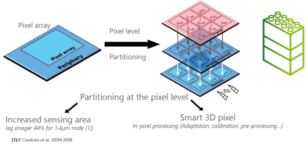
The first industrialization for CoolCube will probably come from smart sensing in a matrix (Figure 7). First applications will be driven by image sensors, µdisplay panels, NEMS mass spectroscopy, biological nanowires sensing or DNA computing. Partitioning the application at the elementary sensing spot increases the sensing area while also permitting a smart 3D in-element processing for sensing adaptation, calibration, pre-processing, etc. CoolCube offers each sensor element to be addressed individually with more than one tiny contact, inducing less parasitic effect, better signal development and optimization between the analog and the digital stages.
Lastly, CoolCube will be one of the major enablers to allow Leti to develop a multi-thousand qubits processor in the next ten years, based on the CMOS silicon spin technology developed by the Grenoble team including CEA Leti, CEA Inac and CNRS Néel Institute. Much less advanced than the superconducting devices, silicon spin qubit reveals itself to be as performing but much more scalable thanks to VLSI 300mm process integration. Then, the only way to conceive a system architecture for a quantum processor is to use 3D technology, at a pitch density level made possible by using CoolCube 3D sequential integration.
About the Author
 Jean-Eric Michallet manages the Microelectronics Components Department at CEA-Leti, covering advanced CMOS, advanced non-volatile memories, mask & PDK, models/simulations, and test/characterization activities. He joined CEA-Leti in 2013 as Microelectronics Business Development Manager after a 20-year career in technical and management positions at Altis Semiconductor and IBM Microelectronics. Prior to joining CEA-Leti, he was a technology transfer officer at the University of Lyon (France). He was a member of the board of Manesman Business Angels, an investment network for high tech start-ups in Paris (France). Jean-Eric Michallet received the M.S degree in Microelectronics from ENSERG Institute (Institut National Polytechnique de Grenoble, France), an Executive MBA and a Master’s degree in International Management from Dauphine University Paris (France)/UQAM Montreal (Canada) and a Management Certificate, Sustainability and Social Responsiveness from ESDES Lyon.
Acknowledgments
Thank you to the following persons from Leti, for their contributions to this article: François Andrieu, Perrine Batude, Laurent Brunet, Séverine Chéramy, Gérald Cibrario, Claire Fenouillet, Richard Fournel, Xavier Garros, Didier Lattard, Sébastien Thuriés, Maud Vinet
Editor’s Note
This article first appeared in its entirety in 3D InCites: The First Decade. Download the digital version here.