June and July have been busy months from a semiconductor conference perspective. VLSI, IITC, imec IFT America, CEA-Leti Innovation Days, MEPTEC, and SEMI’s Innovation for a Transforming World event were all held in roughly a 4-week period. It’s easy to see why a lot of folks are starting to get Zoomed out! One key takeaway, uttered by Leti’s Emmanuel Sabonnadiere before heading to Soitec, is that hardware is back. Without hardware, there is no software!
The conferences were very timely. There has been a great deal of discussion lately regarding the need for the United States and Europe to return to semiconductor and manufacturing leadership in an industry that has gone global. The conferences highlight that technology and technology advancements are now worldwide. Technology that has been developed in the United States, Japan, Europe or Taiwan is to a certain extent manufactured worldwide. In many instances, chips that are manufactured in the United States, or Europe, are packaged in Asia, and then the systems are also assembled in Asia before shipping out to destinations worldwide. Dell, for example, assembles systems in seven factories worldwide: Ireland, Brazil, China, Malaysia, and the United States.
imec ITF and LETI Innovation Days
imec and CEA-Leti are two examples of how research and development (R&D) has also been globalized. Back when high-k metal gates were being explored, I asked a senior technologist at a U.S. logic company why they were working closely with IMEC and CEA-Leti on research projects. One of his responses was, that it is too risky to go it alone and perhaps go down the wrong path. Through collaboration, the respective companies could determine if the technology was feasible and then implement it when the timing was right for their roadmap.
At imec ITF, and Leti Innovation Days, the research consortia give a peek into what they are focusing on from a research perspective. IMEC ITF USA, which typically kicks off SEMICON West week, was held in mid-June followed by Leti Innovation Days later in June.
For those who are not familiar with imec and Leti, they are two of the semiconductor industry’s leading research consortia. imec, in Belgium, has been instrumental in driving gate all around (GAA) transistors, and extreme ultraviolet (EUV). Leti, in France, is known for developed silicon on insulator (SOI) processes. It has also contributed a great deal of work on 3D packaging and transistor technology.
The work performed at both of these institutes is leading edge and has been instrumental in driving the industry’s technology roadmap or both the front- and back-ends. Many of the major semiconductor companies, Intel, TSMC, ST Microelectronics, Samsung, and Hynix have partnered with either imec or CEA LETI on different programs.
IFT USA 2021
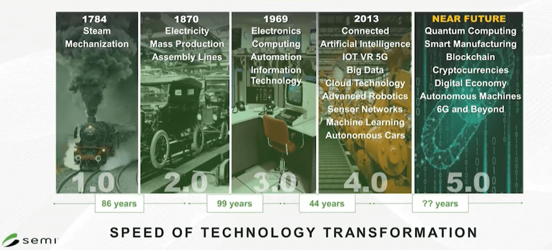
At ITF USA, imec presented on work they are performing in-house with their partners. As in most ITF meetings, Luc Van den hove led off with an overview of the problems imec is focused on addressing and the macro issues facing the world: Pollution, climate, health, and the food shortage. Van den hove touted that imec has been in existence since 1984 and has and will continue to work on semiconductor technology two to four years in advance of production. Before getting down to semiconductor technology Van den hove discussed the macro view of where the electronics industry has been and where it is going (Figure 1)
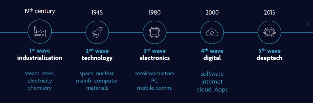
Deeptech, the fifth wave, combines hardware, artificial intelligence (AI), nanotechnology, and molecular engineering. By addressing the fundamental challenges and technology convergence, we will enable deeptech.
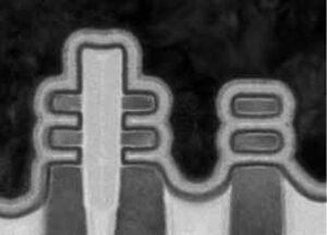
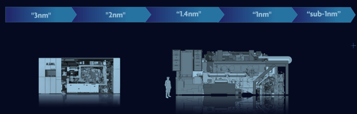
Two of the key areas imec is focused on is high NA EUV that will be needed as the industry starts to shrink below what is referred to as the 2nm technology node, and the extension of nanosheets into forksheet transistors. The forksheet transistor is an extension of nanosheet technology, that essentially folds the P and N transistors up next to each other with a dielectric spacer between them (Figure 2). It improves the transistor density and has the potential for slightly lower power consumption, according to Naoto Horiguchi of imec who presented the imec paper at the VLSI conference.
However, building the forksheet transistor requires advancements in EUV. imec has been one of the primary development areas for EUV lithography and was instrumental in helping ASML get the EUV tool ready for production. This work will continue with a new high NA lab. According to Van den hove, the high NA tool needs to be in production by 2026. Most semiconductor manufacturers will likely participate in this effort using imec as their base for EUV advanced research, before embarking on their own high NA project.
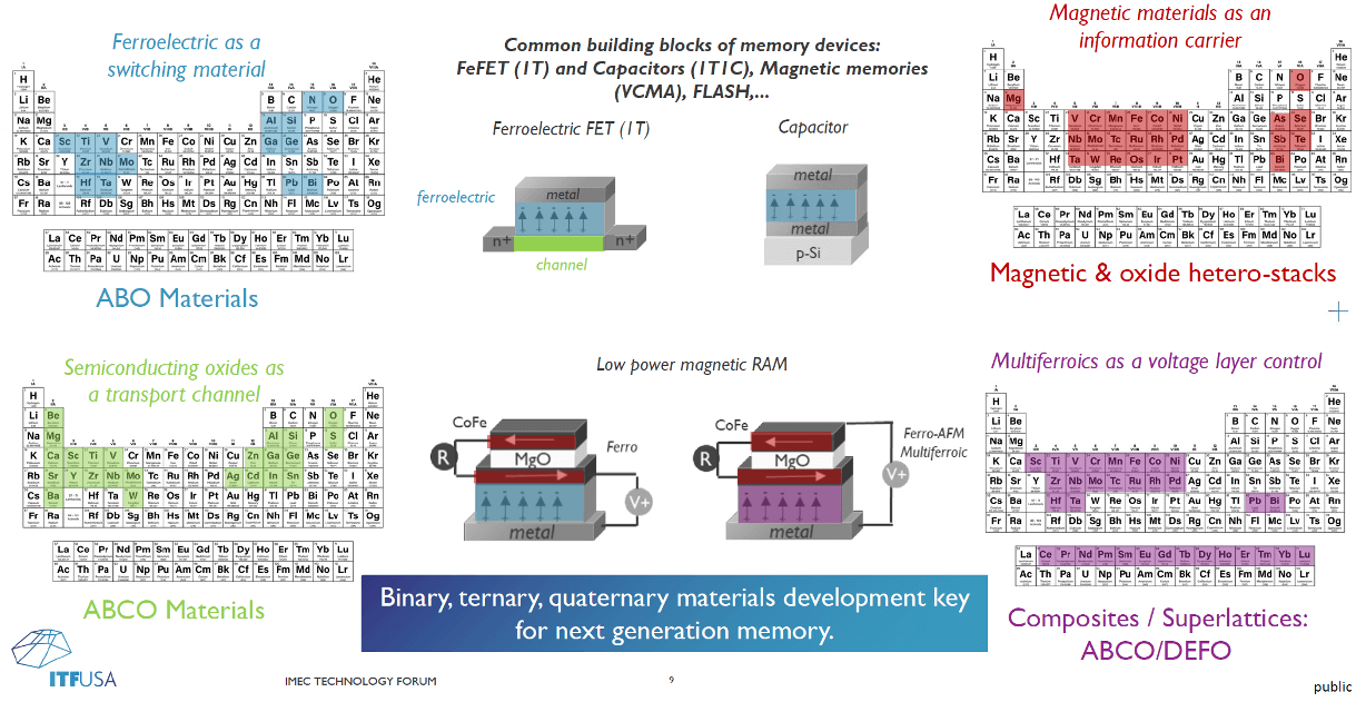
Also from imec, Steven Scheer discussed the evolution of material research to find new materials for gates, interconnects, and insulators. He talked about using AI to weed through all of the possibilities that might work to help improved transistor and interconnect performance. AI could help companies reduce the amount of time researching materials, help in experimental design, and speed time to market (Figure 4).
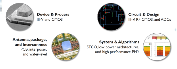
Nadine Collaret then discussed the path to 6G, which will be a necessity for transferring data in the future. She explained how silicon III-V and antennas will need to advance and be packaged to meet the data transfer requirements in the near future (Figure 5).
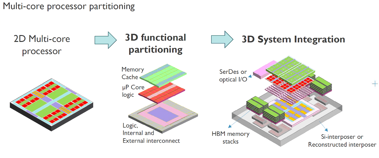
Lastly, Eric Beyne discussed how 3D packaging is needed to remove the memory wall, the access to data, and heat removal from the power wall (Figure 6). The heterogeneous packaging space is extremely active at the moment. The key is being able to combine the chips you need in the same package with a small enough form factor and good interconnect. One of the key challenges is reducing the bump pitch from 50µm to 5µm, and then shrinking further.
ITF USA wrapped up with a panel that included Luc Van den hove, Tim Archer, president and CEO of Lam Research; Peter Wennink, president and CEO of ASML Holding NV; James Thompson, Executive VP of Engineering and CTO of Qualcomm; and Lip-Bu Tan, CEO of Cadence.

The group was asked several questions. The ensuing discussion was interesting. The group considered collaboration to be key to the continued success of the industry. Wennink stated that it was important to not break up the ecosystem and the global collaboration that has been created over the past 60 years. The other speakers alluded to this in one way or another.
Collaboration on a worldwide scale is key to solving the chip technology challenges, supply chain challenges, and the data and energy challenges facing the industry. If any single area gets cut off or cut out it will likely slow the tremendous progress the industry has made over the past decades.
CEA-Leti Innovation Days – Hardware is Back
CEA-Leti presented itself in a slightly different manner. Whereas imec had imec projects as the focus, concluding with a panel discussion with collaborative, Leti had three partners present on issues that were key to them, and how the Leti partnership was moving those projects forward.
Jean-Marc Chery, president and CEO of ST Microelectronics, discussed ST’s and Leti’s efforts in smart mobility, power and energy, IoT, and 5G. Chery took a green approach and discussed the energy footprint of each of these segments, and how developing electric vehicles (EVs), and the use of wide bandgap semiconductors could reduce the CO2 footprint in the automotive space. In IoT, using smart sensors, and better intelligence buildings could lower their energy consumption by using smart lighting and smart HVAC.
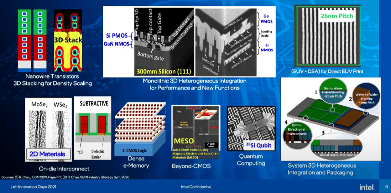
Ann B. Kelleher, senior vice president and general manager of technology development at Intel Corporation, discussed the technology challenges facing the industry as the world becomes digital. She mentioned that in 2000 there were more than 15 companies competing at the leading edge in logic. Now there is just a handful. Kelleher shared the industry technology roadmap for transistors, compute and packaging, and how Intel and Leti are partnering in solving some of the challenges in the 3D packaging space (Figure 8).
The industry speaker was Ajit Manocha, president and CEO of SEMI. Manocha discussed the transformation of the industry over the years, and how the semiconductor industry was still growing and innovating, and the importance of collaboration in the worldwide industry (Figure 9).
Manocha also discussed SEMI’s role in setting standards and roadmaps and highlighted the recent heterogeneous integration roadmap that SEMI put together
As mentioned at the beginning of the article, Lastly Emmanuel Sabonnadiere closed out the session with Hardware is Back! The industry needs to figure out how to balance the compute power and memory, as more and more devices get connected.
The software doesn’t exist without hardware, and great hardware will be needed to help the world combat the energy challenges that are facing us in the future.