3DIC Integration using 3D stacked technologies in its true definition has a long history.1 Richard P. Feynman expressed this vision in 1985: “Another direction of improvement of computing power is to make physical machines three-dimensional.”2 Successively, several research and development (R&D) initiatives started world-wide. In the late 1980s, in a German consortium comprising Siemens, Philips, and Fraunhofer Munich, 3D CMOS test devices as 3D SRAMs were realized based on recrystallization of thin Si.3 Such monolithic concepts are reconsidered today as “the ultimate 3D” for stacking at transistor level — in the International Roadmap for Devices and Systems (IRDS) for the 2030s.
Early 3D Stacked Developments
Towards the end of the 1990s, Mitsumasa Koyanagi´s team at Tohoku University succeeded in fabricating 3D ICs using through-silicon vias (TSVs) to create 3D stacked image sensors and 3D stacked memory test chips.4 This represented the pioneering contributions of today´s two key applications in high volume production.
Simultaneously, Fraunhofer in Munich was focused on the key application of heterogeneous systems, consisting of components with different materials/technologies and die sizes. Robust die-to-wafer stacking technologies were developed to achieve what is now called 3D heterogeneous integration.3,5
But despite these early demonstrations, it wasn’t until 2015 that Samsung produced a high volume 3DIC product; stacked DDR4 and later second-generation high bandwidth memory (HBM2) memory. CMOS image sensors also went into high-volume production. In 2017, Sony ramped the production of stacked CMOS image sensor (CIS) for smartphone cameras. Even so, there were setbacks. Most significantly, 3D memory‐on‐logic applications, widely forecasted by many sources, have been postponed several times.
Why 3D Integration?
Essential driving forces for 3D integration are performance (speed), power consumption, costs, and form factor. While TSV technologies using advanced intermetallic compound (IMC) bonding or hybrid bonding processes provide very high vertical interconnect densities, the major issue is the high manufacturing cost. Nevertheless, TSV technology shows up as packaging mainstream for high-performance 3DICs. However, alternative concepts “between 2D and 3D” were very successful for products with no need of such high interconnect performances, i.e. Si interposer technology. And moreover, alternative interposer concepts avoiding costly TSV technology are gaining importance, as e.g. Intel´s omnidirectional interconnect. Figure 1 shows all of the 3D stacked technologies available today.
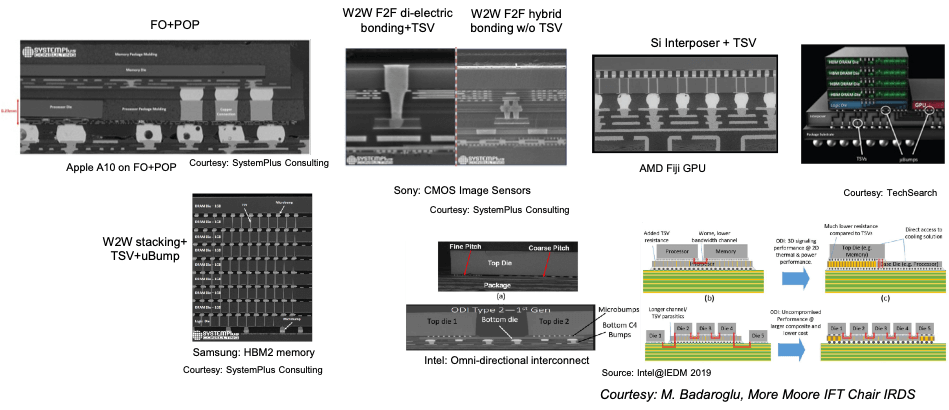
The Heterogeneous Integration Roadmap has defined corresponding architectures between 2D and 3D. As examples, TSMC´s CoWoS and Intel´s EMIB6 are categorized as 2DS architectures, Inactive Si, with TSV and without TSV, respectively.
Dis-Integration is Underway
We have known for some time that with lateral scaling slowing down, the industry would need to find another way to continue to move forward. One of the options being implemented is to actually “disintegrate” SoCs into their functional parts and then connect these “chiplets” back together on high-density interposers.
Building complete circuits from pre-verified chiplets is gaining traction as a way of cutting costs and reducing time to market for heterogeneous designs. Chiplets allow us to use the latest node only where needed which in turn results in reduced silicon cost. These silicon savings, in turn, can be allocated for more expensive packaging solutions.
AMD, Intel, and TSMC have all introduced or announced chiplet-based products and/or technologies. It is also widely accepted that mixing and matching chiplets produced at different foundries will require standard interfaces and communication protocols. This is currently the most important thing we can do to stabilize and broaden the chiplet infrastructure. The hope is that these functional chiplets will create a library and in the future, we can combine these tested chiplets from multiple foundries to devise future circuits.
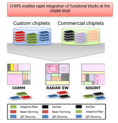
The US Department of Defense (DOD) Defense Advanced Research Projects Agency is in year four of its Common Heterogeneous Integration and IP Reuse Strategies (CHIPS) program, which has been looking at chiplet based solutions for the military (Figure 2).
Chiplet Physical Interfaces
A key enabling technology is a chiplet-to-chiplet interface. There are several layers to such an interface including protocol and physical layers. The ideal physical layer interface would achieve the power and area footprint of a long-range on-chip SOC driver/receiver pair while enabling a high aggregate bandwidth, being able to drive a wide range of wire lengths (with the attendant range of line losses), and support standardized design-for-test (DFT). Key decisions include voltage swing, serialization, clock management, bus-widths, etc.
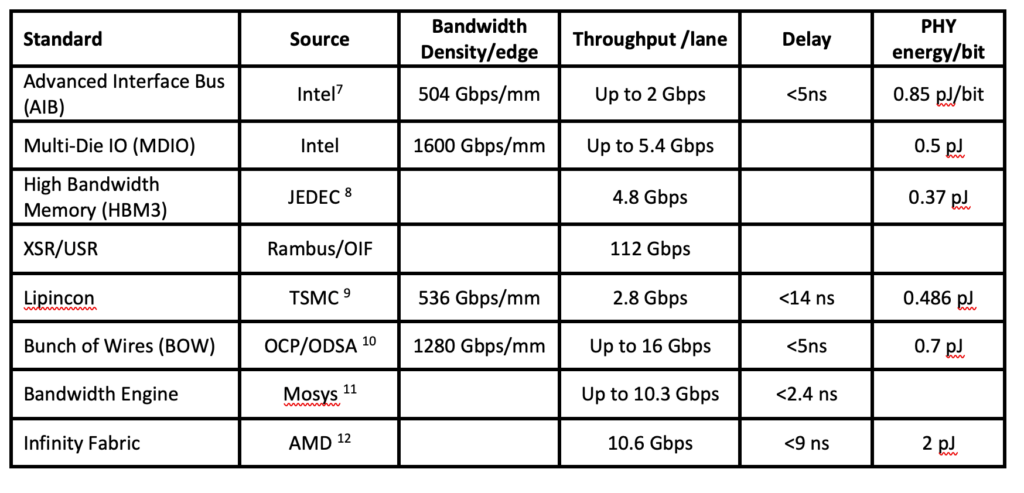
A number of chiplet interfaces have been proposed. These proposals and some salient features are summarized in Table 1.
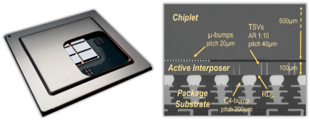
Chiplet Integration onto Active Interposers
Large-scale interposers for chiplet integration have been fabricated using various technologies, such as 2.5D passive interposers, organic substrates, and silicon bridges. These technologies are mature with economic benefits, but still raise limitations. Due to wire-only interconnects, inter-chiplet communication is still limited to side-by-side communication reducing the number of connected chiplets; the passive interposers cannot carry any functions; and finally, co-integration of chiplets with incompatible interfaces is impossible.
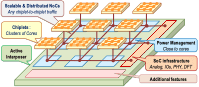
To tackle these issues, the concept of the active interposer is introduced by integrating some active CMOS circuitry on a large-scale interposer. The active interposer can be seen as a generic bottom die infrastructure which integrates i) flexible and distributed interconnect fabrics for scalable chiplet traffic, ii) energy-efficient 3D-plugs using fine pitch interconnects, iii) power management feature for power supply closer to the cores, and iv) memory-IO controller and PHY for off-chip communication. Finally, the active interposer integrates 3D DFT to enable known-good-die (KGD) strategy. Being of low computing complexity and reduced power budget, the active interposer does not exacerbate the thermal issues of the 3D device.
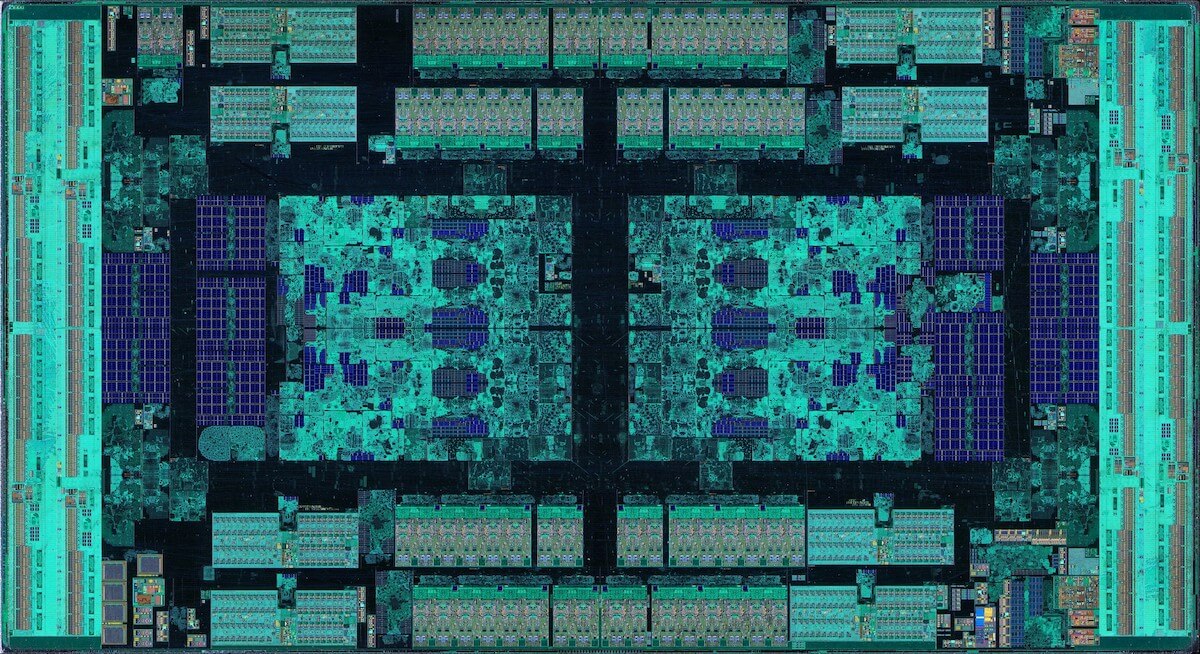
As an active interposer prototype,13 the IntAct circuit is composed of six identical chiplets (28nm FDSOI) each integrating 16 cores, 3D stacked with fine-pitch (20μm) micro-bumps on an active interposer (65nm CMOS) using TSV middle (Figure 3). The active interposer integrates distributed interconnects for low latency long-distance communication, 3D-plug achieving 3 Tbit/s/mm2 bandwidth density and fully integrated switched-capacitor voltage regulators. The circuit implements a total of 96 cores with a scalable cache-coherent architecture, delivering a peak 220 GOPS. Thanks to this partitioning and 3D fine pitch, users get more GOPS at the same power budget and benefit from an increased memory-computing ratio along the memory hierarchy.
As mentioned in the above section, 3D communication standards are strongly required to enable true chiplet compatibility, active interposer is however a solution enabling to bridge incompatible chiplets by integrating ad-hoc bridge logic.
![[err-ad-fallback-title]](http://www.3dincites.com/wp-content/plugins/a3-lazy-load/assets/images/lazy_placeholder.gif)
For energy-efficient computing, chiplet-based partitioning and 3D technology are driven by two main trends:14 heterogeneity (as presented in reference 15) and pitch reduction for energy-efficient interconnects for increased coupling between memory and computing. 3D pitch reduction will continue thanks to hybrid bonding technology applied to chiplet integration, with reduced pitches (10µm and targeting below).16
Architectures between 2D and 3D are best tailored for the different specific heterogeneous applications. The different applications, as e.g. memory, CMOS image sensor, GPU, radio frequency ICs (RFICs), and chiplet-based products need best-tailored technology solutions for their specific performance, power consumption, costs, and form factor requirements.
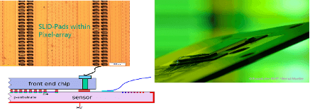
Besides 3DIC integration in its strong definition, a variety of architectures between 2D and 3D are potentially well-suitable for cost-effective production. This is especially true for the growing market of heterogeneous 3D sensor/IC systems with the need for robust die-to-wafer stacking of components of significant different device technologies, as CMOS, sensors, actuators, and MEMS17,18 rather than extremely small TSV/pad pitches.
A corresponding example of heterogeneous 3D sensor integration is shown in Figure 4. The photon detector and appropriate read-out IC are 3D integrated by intermetallic compound (IMC) bonding with mechanically stable Cu/Sn Solid-Liquid-InterDiffusion (SLID) interconnects 18.
To pay more attention to the described fine-pitch stacking concepts and new architectures “between 2D and 3D”, the IEEE EPS Technical Committee 3D decided to broaden its objectives from 3DIC and monolithic integration on one side, to non-TSV 3D technologies, chiplet assembly, Si interposer, and alternative interposer concepts (including TSV less), on the other side of the fine-pitch interconnect “spectrum”.
Visit our website for information on TC 3D/TSV.
This article originally appeared in the 2021 Yearbook. Read the issue online here.
Contributing Authors

Mustafa Badaroglu, Ph.D., is Principal Engineer at Qualcomm responsible for technology and architecture development for products employing compute-In memory technology. He previously worked at Huawei, Qualcomm, IMEC, ON Semiconductor, and Tubitak. Badaroglu is the global chair of the IRDS More Moore Team focusing on the high-volume manufacturing roadmap of logic devices and memory. He is a senior member of
IEEE.

Paul D. Franzon, Ph.D. is currently the Cirrus Logic Distinguished Professor and the Director of Graduate programs in the Department of Electrical and Computer Engineering at North Carolina State University. Paul has also worked at AT&T Bell Laboratories, DSTO Australia, Australia Telecom, Rambus, and four companies he co-founded — Communica, LightSpin Technologies, Polymer Braille Inc., and Indago Technologies. His current interests include applying machine learning to EDA, building AI accelerators, neuromorphic computing, RFID, advanced packaging, 2.5D and 3DICs, and secure chip design. Paul has led several major efforts and published over 300 papers in these areas.

Philip Garrou, Ph.D., is a subject matter expert for DARPA and runs his own consulting company, Microelectronic Consultants of NC. He is well known for his weekly advanced packaging blog, Insights from the Leading Edge. Since retiring from Dow Chemical, Phil has served as Technical VP and President of both IEEE EPS and IMAPS and is a Fellow of both organizations. He has edited several microelectronic texts and won multiple industry awards.
 Pascal Vivet is Scientific Director of the Digital Systems and Integrated Circuits Division in CEA-LIST, Grenoble, France. He received his Ph.D. from Grenoble Polytechnical Institute in 2001, designing an asynchronous microprocessor. After 4 years within STMicroelectronics, he joined CEA-Leti in 2003 in the digital design lab. His research interests cover wide aspects of circuit and system-level design, ranging from system integration, multi-core architecture, Network-on-Chip, energy-efficient design, related CAD design aspects, and in strong links with advanced technologies such as 3D integration, Non-Volatile-Memories, photonics. He was project leader on 3D circuit design and integration since 2011. He participates to various TPC such as ASYNC, DATE, 3DIC, ISLPED conferences. He served as a member of the organizing committee of the 3D workshops series at DATE from 2013 to 2015, and to the D43D workshops since 2011, and to the 3DIC conference. He has authored and co-authored more than 120 papers and holds several patents in the field of digital design. He is a member of IEEE.
References
- Handbook of 3D Integration “Technology and Applications of 3D Integrated Circuits”, edited by Philip Garrou, Christopher Bower, Peter Ramm, Wiley & Sons (2008).
- Richard P. Feynman «The computing machines in the future», Nishina Memorial Lecture at Gakushuin University (Tokyo) (1985).
- Peter Ramm et al. «3DIC: Past, Present and Future – a European Perspective», Plenary Talk at 2020 IEEE 70th Electronic Components and Technology Conference (2020).
- Mitsumasa Koyanagi et al., IEEE IEDM Tech. Digest, pp. 879-882 (1999).
- Peter Ramm et al., Japanese Journal of Applied Physics 43 (7A), L 829 (2004).
- Ravi Mahajan et al. «Embedded Multi-Die Interconnect Bridge (EMIB)», 2016 IEEE 66th Electronic Components and Technology Conference (2016).
- David Kehlet, “Accelerating Innovation Through A Standard Chiplet Interface: The Advanced Interface Bus (AIB),” Intel White Paper retrieved from https://www.intel.com/content/dam/www/public/us/en/documents/white-papers/accelerating-innovation-through-aib-whitepaper.pdf
- H. Ko et al., “A 370-fJ/b, 0.0056 mm2/DQ, 4.8-Gb/s DQ Receiver for HBM3 with a Baud-Rate Self-Tracking Loop,” 2019 Symposium on VLSI Circuits, Kyoto, Japan, 2019, pp. C94-C94, doi: 10.23919/VLSIC.2019.8778082.
- Mu-Shan Lin et al., “A 16nm 256-bit wide 89.6GByte/s total bandwidth in-package interconnect with 0.3V swing and 0.062pJ/bit power in InFO package,” 2016 IEEE Hot Chips 28 Symposium (HCS), Cupertino, CA, 2016, pp. 1-32, doi: 10.1109/HOTCHIPS.2016.7936211.
- S. Ardalan et al., “Bunch of Wires: An Open Die-to-Die Interface,” 2020 IEEE Symposium on High-Performance Interconnects (HOTI), Piscataway, NJ, USA, 2020, pp. 9-16, doi: 10.1109/HOTI51249.2020.00017.
- M. J. Miller, “Bandwidth engine® serial memory chip breaks 2 billion accesses/sec,” 2011 IEEE Hot Chips 23 Symposium (HCS), Stanford, CA, 2011, pp. 1-23, doi: 10.1109/HOTCHIPS.2011.7477493.
- B. Kleveland et al., “An Intelligent RAM with Serial I/Os,” in IEEE Micro, vol. 33, no. 6, pp. 56-65, Nov-Dec 2013, doi: 10.1109/MM.2013.7.
- P. Vivet et al., “INTACT: A 96-Core Processor with 6 Chiplets 3D-Stacked on an Active Interposer with Distributed Interconnects and Integrated Power Management”, IEEE Journal of Solid-State Circuits, Volume: 56, Issue: 1, January 2021.
- D. Dutoit, et al., “How 3D integration technologies enable advanced compute node for Exascale-level High-Performance Computing?”, IEDM, 2020.
- Pierre-Yves Martinez et al., “ExaNoDe: combined integration of chiplets on active interposer with bare dice in a multi-chip-module for heterogeneous and scalable high-performance compute nodes”, VLSI Conference, 2020.
- Amandine Jouve et al., « Die to wafer direct hybrid bonding demonstration with high alignment accuracy and electrical yields », IEEE 3D System Integration Conference, Sendai (3DIC 2019).
- Josef Weber, Montserrat Fernandez-Bolanos, Adrian Ionescu and Peter Ramm, « 3D Integration Processes for advanced sensor systems and high-performance RF components », ECS transactions 86 (8), 2018.
- Peter Ramm, Armin Klumpp, Christof Landesberger, Josef Weber, Andy Heinig, Peter Schneider, Guenter Elst, Manfred Engelhardt, « Fraunhofer´s Initial and ongoing contributions in 3D IC Integration», IEEE 3D System Integration Conference, Sendai (3DIC 2019).