Actually, 3D System integration takes more than a village. It takes a global effort. As Virtual ECTC 2020 continues this month, I viewed the 3D Past, Present, and Future of 3D integration Plenary Session. The actual viewing time is just over 115 minutes. The impressive speaker line-up included 3D pioneers, Mitsumasa Koyanagi, Tohoku University; Peter Ramm, Fraunhofer EMFT; Eric Beyne, imec; Paul Franzon, NCSU, and representing industry, Doug Yu, TSMC. All provided their perspectives on the 3D technology journey. Together, they provide an incredible history lesson, in addition to predictions for how 3D system integration plays out on the roadmap. If you are a newcomer to this industry, this is two hours well spent, learning from the very people responsible for making it happen. And it’s free and available until June 30. Register here. Here are some of the key points I took away from the session, lightly seasoned with my own observations and input from other sources.
3D Integration Past
When 3D integration began really depends on who’s doing the talking. I always believed it began around 2006-2007 when the EMC3D Consortium formed to address the through silicon via (TSV) process flow to address technology challenges and reduce the cost to bring them to commercialization. After listening to Koyanagi and Ramm, I realized I couldn’t be more wrong. (Really. This could cost me my crown.)
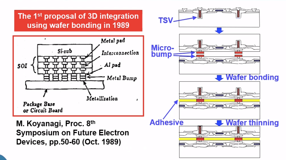
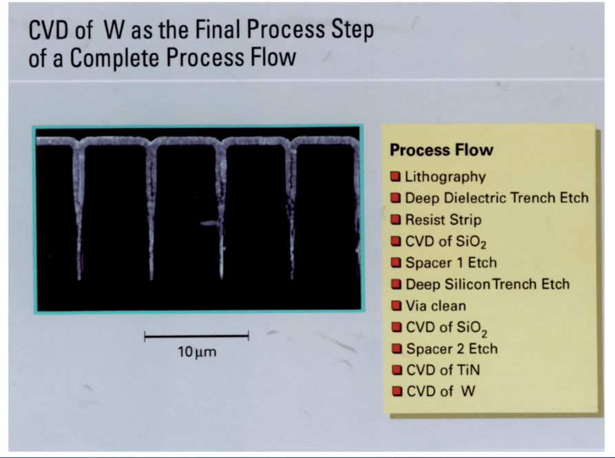
According to Koyanagi, 3D device stacking development began in Japan in 1975 for memory applications such as DRAM, NAND, MRAM, and others. There were also approaches being developed for stacking resistors, CMOS transistors, and 3D transistors (finFETs). The 1980’s brought monolithic approaches using laser annealing, selective epitaxial growth, and wafer bonding. As early as 1989, both Koyanagi and Ramm proposed TSV technology (Figures 1 -3).
Other 3D concepts that got their start at Tohoku University included a 3D stacked multi-core processor with first self-test and self-repair function (2002) and also 3D stacked image sensors (2004-2006).
In Europe, according to Ramm, 3D efforts can be traced back to the late 1980s, with a German research project for monolithic 3D IC involving Siemens, AEG. Philips, and Fraunhofer. And before it was called TSV, interchip via technology was developed using adhesive-based bonding of fully processed device wafers.
It’s clear, the R&D across the world really laid the groundwork for the commercialization of today’s 3D integration technologies.
But What Took So Long?
Since this technology started 45 years ago, why did it take so long to reach commercialization? According to these pioneers, sometimes it was technology limitations that took innovation to solve – such as a process or tool. Other times it was happenstance or some hot competition from an alternative technology.
For example, as Ramm explained, until CEA-Leti came up with CoolCube™ technology and broke through the temperature limitation budget with CMOS cooled activation, monolithic 3D was stalled.
DRAM stacking would likely have been adopted much sooner, had not the ill-fated Quimonda closed its doors in 2008, just after it had qualified TSV with solid-liquid interdiffusion (SLID) bonding for DRAM stacking. It took until 2015 when SK Hynix introduced 3D TSV DRAM stacks for its bandwidth memory (HBM) before 3D memory stacking using TSVs reached volume production.
Another event cited by Ramm that delayed 3D integration going into volume was the success of fan-out wafer-level packaging (FOWLP). This achieved form factor and interconnect density at a lower cost than TSV, displacing the progress of 3D ICs.
In many ways, 3D integration technologies were ahead of their time, looking for applications that couldn’t advance to the next level capabilities without it: CMOS image sensors, memory, and high-performance computing.
Doug Yu, TSMC offered what he called his “narrow-minded opinion of 3D IC”, He says package, performance, power, profile, cost and cycle time (PPPCC) are the key performance indicators (KPIs) for 3D IC technologies. This is true now and always not just past present and future, he said. That’s why we don’t find TSVs in cost-sensitive applications, he says. The goal is to get good systems PPPCC.
“TSV is not yet popular for mobile because of technology challenges and cost,” said Yu “It will come to the point of needing it for bandwidth and density. Moving connections into closer proximity is key to achieving high speed and power efficiency. Power consumption is the bottleneck.”
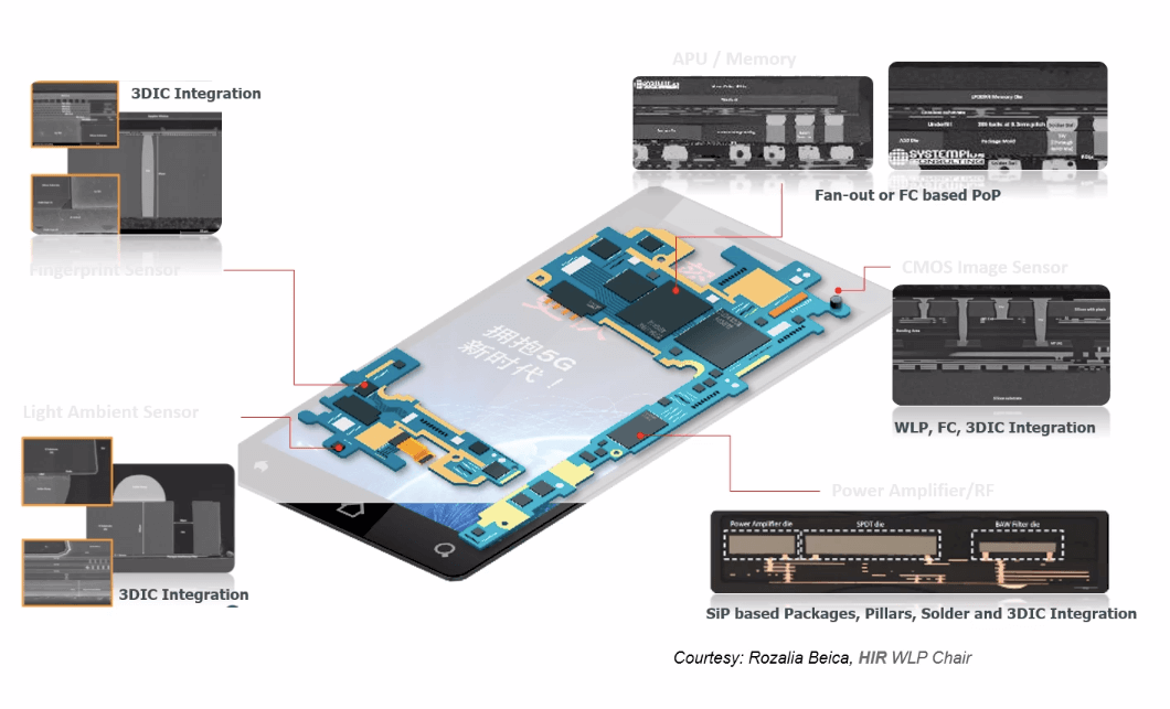
And yet, in Figure 4, presented by Ramm, and provided by Rozalia Beica, we see several 3D ICs using TSVs in smartphones. Ramm showed this because he said smartphones are a good indicator of technologies that are reaching volume production.
3D Enabling Heterogeneous Integration
If you’ve seen it written on 3D InCites once, you’ve seen it a thousand times: today’s drivers like artificial intelligence (AI), 5G, edge computing, and more all require aggregation of different types of technologies in one package.

Beyne used a mobile processor as a good example of this – integrating multi-core processors, on-chip memory, and RF devices. He describes fundamental partitioning as splitting the cache from the logic and moving secondary functions to the bottom die. Partitioning to optimize performance and cost leads to an overall lower cost, he explained. This creates a challenge for electronic design automation (EDA). Herb Reiter blogs about that here.
Koyanagi predicts that 3D IC will evolve into heterogeneous 3D systems. Beyne explained that partitioning a system into different functionalities and then reintegrating them using 3D heterogeneous integration requires an exponential increase in 3D density.
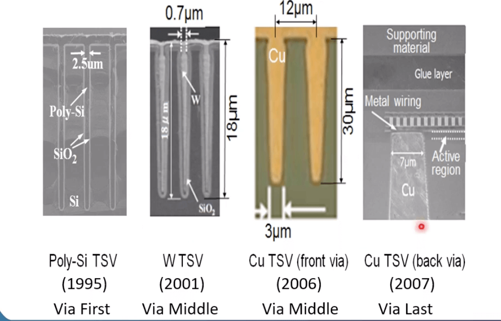
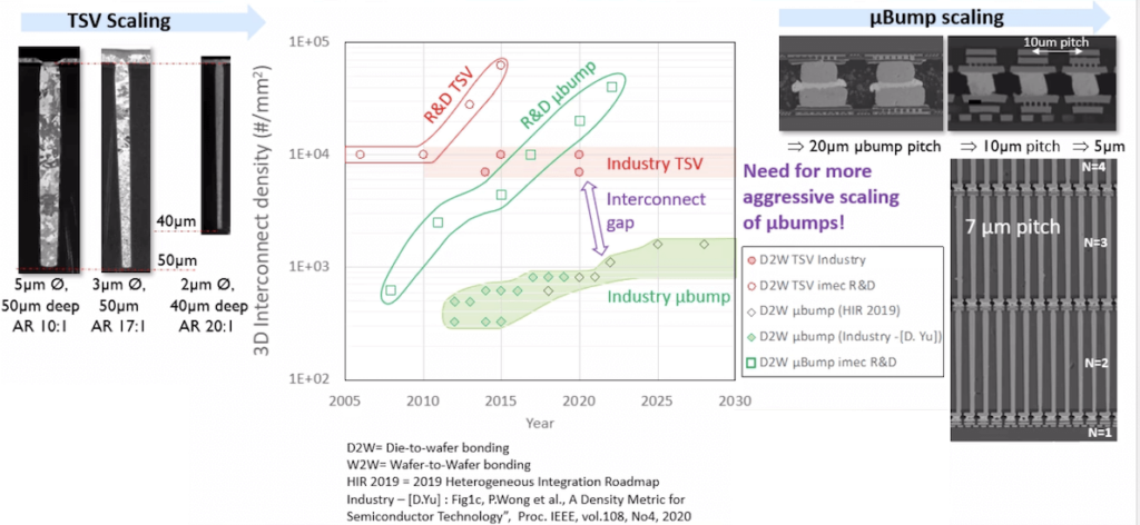
Both Beyne and Yu explained how micro-bump pitches are limiting interconnect density. While TSVs have successfully scaled to 20:1 aspect ratio (2µm x 40µm), microbumps have only achieved 10µm bump pitch when it needs to go to 5, leaving what Beyne calls an interconnect gap. He said there is a need for aggressive micro-bump scaling, which is currently in R&D at imec (Figure 5).
Hybrid Bonding Holds the Key
So how do we bring layers closer together and making interconnects shorter to bridge the interconnect gap? Whether you’re TSMC and call it system on interconnect chip (SoIC) or everyone else and call it hybrid bonding – it appears to be the key to unlocking high density interconnect.
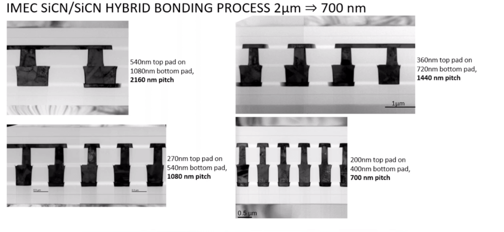
Wafer-to-wafer hybrid (W2W) bonding approaches have been used in volume production of CMOS image sensor (CIS) technology for some time. Die-to-wafer (D2W) hybrid bonding is also reportedly now ready for volume production. The challenge now is achieving finer pitches with each of these processes to eliminate the TSV/micro bump pitch gap.
Currently, W2W approaches achieve 1µm pitch, and die-to-wafer achieves 5µm pitch. To keep up with CMOS scaling, Beyne says we will need to see 0.5µm pitches for W2W and 3-5µm pitches for D2W or D2D. And since research to commercialization is generally a 5-10 year cycle, he believes we will see both in the next 10 years (Figure 6).
To me, that seemed like a long time. So, I checked in with Xperi’s Laura Mirkarimi, who is currently leading efforts for the company’s D2W hybrid bond technology DBI Ultra™, which is based on its well established DBI™ process for W2W hybrid bonding.
While she agrees with Eric in general, Mirkarimi says she doesn’t think it will take 10 years to get there. “The clocks have started and there are companies making that structure size (0.5µm) now,” she said. “The market will always have leapfrog companies willing to go out on a limb and focused improved technology to offer advanced applications in the next generation of devices. For example, Sony leapfrogged the competition with image sensors when it took on hybrid bonding, solved yield-related issues while building a foundation for 3D integrated architectures.”
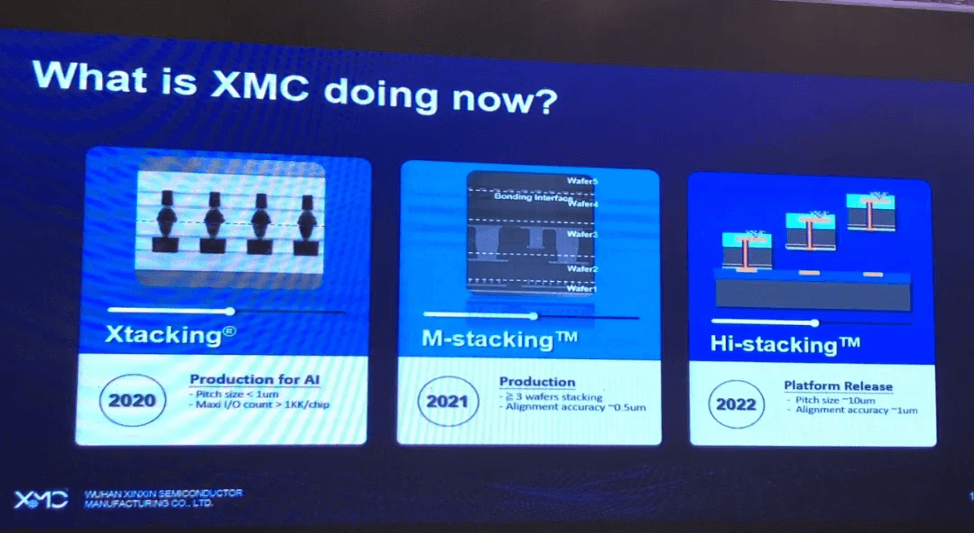
She said accelerated development can also be influenced by manufacturers’ pain points. Some companies are focused on current product releases and maybe addressing today’s challenges. For example, since 2019 Chinese manufacturer YMTC’s hybrid bonding 64L product has been in production, and the company is talking about rolling out its 128L-layer 3D NAND product that uses W2W to achieve sub-micron pitches later this year. YMTC can do this because it recently acquired XMC, a 300 mm fab in Wuhan that in 2006 collaborated with OmniVision to build its CIS technology using 3DIC. OmniVision is a licensee of Xperi’s ZiBond and DBI technology. YMTC calls its hybrid bonding Xtacking and is in production with a sub-micron pitch AI chip. (Figure 6)
Mirkarimi says in D2W stacking, the industry’s pain points are yield and performance in HBM. While the interconnect pitch here is determined by the TSV pitch, she believes D2W stacking at 3-5µm pitches could happen in the next 2-5 years.
“We’ve developed our hybrid bonding technology that is compatible with existing toolsets for ease of adoption in D2W package assembly lines,” she said. “We offer a full tech transfer package including process optimization and design rules We know how to do it.”
The Future is 3D System Integration
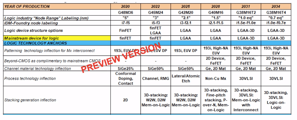
If this preview version of the 2019 IEEE IRDS Logic Device Roadmap is anything to go by, 3D system integration via W2W and D2W stacking is set to roll out in 2022 (Figure 7). All the 3D integration pioneers agree on one truth: 3D system integration is going to take everything in our 3D technology arsenal to come to life. It took us 45 years to get this far, but we’ve done it. Let’s see how far we can take it now. ~ FvT