Combines Siemens’ EDA expertise and software with NVIDIA AI infrastructure and software to improve result quality, time-to-results, tool-calling reliability and...
Wafer cleaning is one of the most critical steps in the semiconductor process flow, especially as dimensions continue to shrink to below the 1-nanometer (nm) node. Photoresist residue and particulates can...
The semiconductor industry finds itself at a critical juncture, where the traditional paradigms of Moore’s Law are encountering fundamental physical...
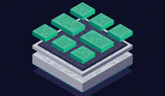
As the industry pushes toward ever-greater levels of semiconductor performance, integration and efficiency, the promise of 3D integrated circuits (3D...
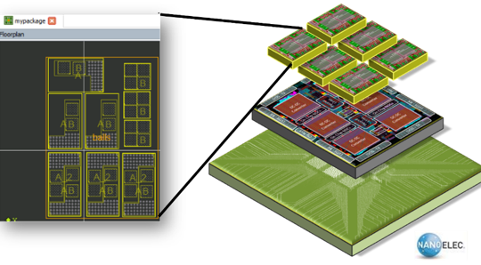
Understanding the role of compromises and trade-offs in the design process Electronic packages serve many purposes including protecting, connecting, and...