
When planning the 24th EDPS, the organizing committee, chaired by Shishpal Rawat, former Intel executive, took a number of bold steps
- EDPS was traditionally held in the spring. We moved EDPS to the fall because that’s a time when more new IC projects are being planned.
- After many years of holding it in Monterey, we moved EDPS to Milpitas to make it more easily accessible for Silicon Valley folks.
- While conceived as an Electronic DESIGN Process Symposium, we invited, in addition to EDA and IC design experts, many presenters and panelists from IC MANUFACTURING companies, because more and more of the IC value creation and differentiation is moving to IC packaging. This makes the IC manufacturing backend much more challenging and requires closer IC design and manufacturing cooperation.
- Last, but certainly not least, instead of hosting the event at an expensive Silicon Valley hotel, we got the support of SEMI, the IC manufacturers’ powerful industry association, to host EDPS 2017 at their impressive headquarters in Milpitas. This allowed us to keep our cost down and pass the savings on to EDPS attendees.
- Looking at so many moving parts, you may think “Oh, boy, this event must have gone terribly wrong!”
To the contrary! Compared to previous years, twice as many industry executives attended EDPS 2017, presented thought-provoking subjects, contributed to interesting discussions and enjoyed valuable networking opportunities between IC design and manufacturing experts.
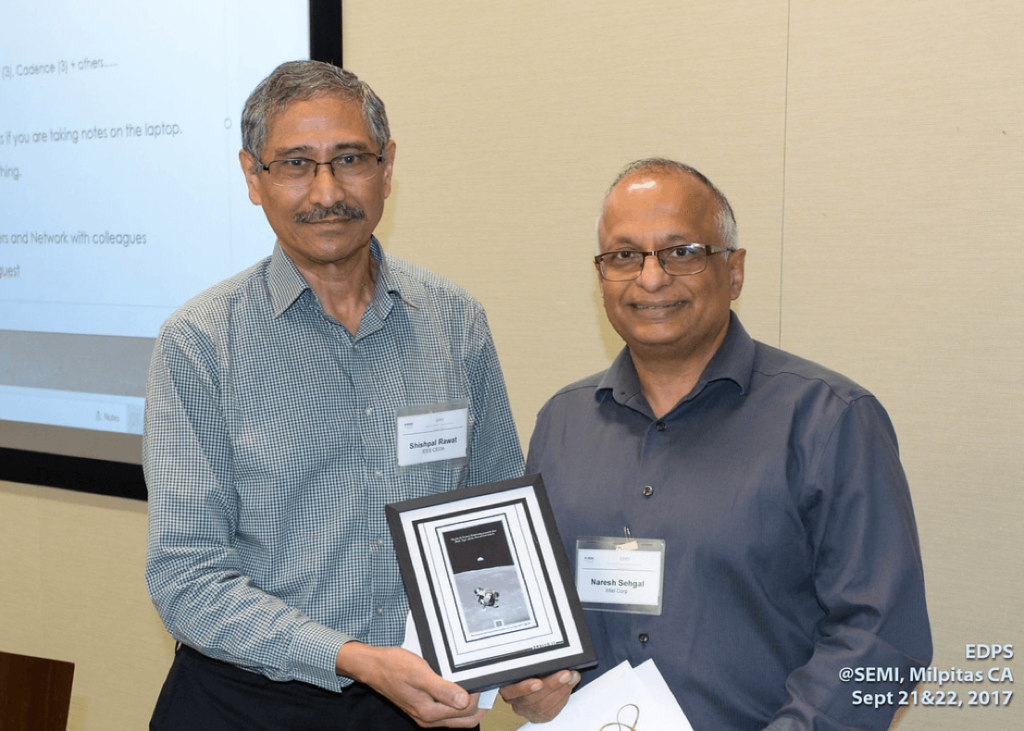
At the end of this successful conference, Intel’s Naresh Sehgal, an avid EDPS supporter for many years, presented Shishpal Rawat, our hard-working committee chair, a very telling award for turning, what some saw as a Moon Shot, into a successful industry conference:
SEMI demonstrated the IC manufacturers’ interest in working with EDA and IC design experts, not only by hosting EDPS in their facility. Together with Rawat, our conference chair, Dave Anderson, SEMI’s President of the Americas, welcomed the attendees, then outlined SEMI’s many roles, and highlighted the steadily increasing importance of good communication and cooperation across the entire IC supply chain.
Enough said about the conference in general. Let’s look at the technical content and the individual sessions of this one-and-a-half-day event.
Our first keynoter was Antun Domik, Synopsys’ CTO. He conveyed the largest EDA vendor’s many strengths in support of smaller and smaller feature sizes, outlined the industry’s progression from planar transistors to FinFETs and gate-all-around devices and mentioned that 5.5D ICs (= 3D-ICs, e.g. HBMs, mounted on a “2.5D” interposers), are bound for success.
After a short break, Naresh Sehgal introduced this session’s speakers: Rajesh Gupta from UCSD, John Lee from Ansys, CP Hung from ASE and Bill Bottoms from 3rd Millenium Test Solutions. They all highlighted the importance of design tools and offered ideas for better methodologies and tools for IC design and manufacturing to get ICs to market faster.
For me, the highlight of this conference was Zoe Conroy’s keynote, right after lunch. As a senior manager at Cisco, Conroy lives in both the IC design and manufacturing world. She directs the engineering teams working on design-for-test (DFT) and the production test floor. Conroy presented several key challenges her teams work on regularly, before a highly reliable Cisco switch, router or other networking equipment can be shipped to customers. Like other speakers, Conroy asked for better communication and cooperation across the supply chain. Specifically, she highlighted the importance of detailed traceability info for every component, all the way back to its originator(s). In addition, Conroy asked for improvements at system-level test (SLT). This step should consider more of the environmental factors of the real application, and with it catch more defects, before components reach the board and system test stages.
Conroy suggested to define traceability standards, or at least best practices, to pinpoint the reason for a board or system failure faster and accelerate production ramp-up. Only when a system passes all the stringent tests, it can be shipped and earn revenue.
The following session was titled “driving to higher yield”. Like Sehgal in his morning session, I was also able to mix design and manufacturing topics by winning Keith Arnold from PDF Solutions, Asim Salim from Open-Silicon, HC Peng from ASE and Juan Rey from Mentor, a Siemens Business, as presenters. All four outlined what kind of yield challenges they see and how their products and/or services contribute to improving yield and lowering unit cost.
The next session focused again on a topic where design and manufacturing experts need to work together to make a difference. Intel’s John Swan and Priyardarsan Patra had invited Gajinder Panesar from UltraSoC, Cynthia Cook from Intel, Al Czamara from TestEvolution and Vikas Kumar, also from Intel, to present how they accelerate product debug and validate component quality.
Another highlight of this long day was Jim Hogan’s dinner keynote: “The Fourth Industrial Revolution. The Cognitive Era.” In a somewhat noisy environment at the nearby Embassy Suites in Milpitas, Hogan presented a lot of data point about our current environment and reasoned why and how these facts are impacting us today and may change our lives in future.
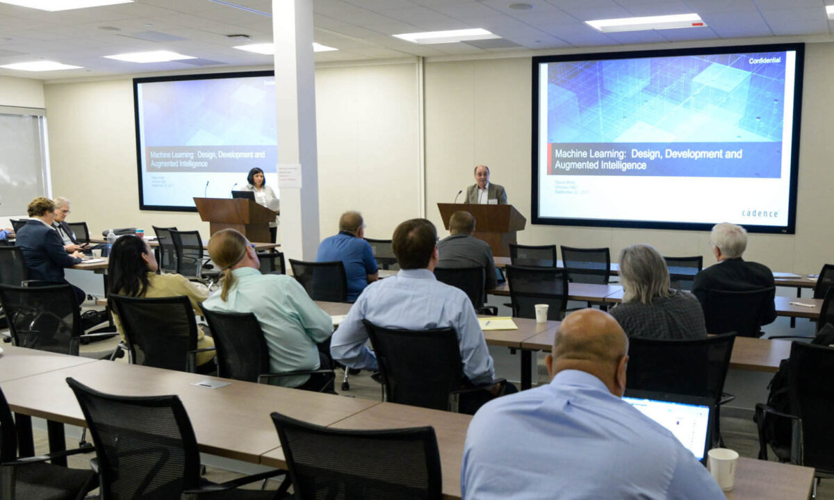
On Friday EDPS traditionally focuses on a current and very hot topic. This year it was: “Machine Learning (ML), Applied to IC Manufacturing and Design.” After a very visionary keynote from Western Digital’s Pankaj Mehra, Aparna Dey from Cadence introduced her presenters: Paul Franzon from NCSU, David White from Cadence, Rob Aitken from ARM, Jeff Dyke from Solido and Abhijit Chatterjee from GeorgiaTech. They not only taught us the ML basics but also outlined why and how this rapidly emerging technology is gaining importance in both IC design and manufacturing.

During my years at EDA companies, I often heard complaints about how unfair ASIC design and manufacturing companies were because most of them only spent two percent (2 %) of revenue on EDA design tools. After I founded my own company, eda2asic Consulting, Inc., I analyzed this point more closely and realized that all these companies spent about ten times as much money on capital equipment for their manufacturing groups as they invested in EDA tools for their designers. If EDA companies can also make IC manufacturing and test groups more productive, they should be able to break through this “2% glass ceiling”!
That’s why I pushed hard to get many manufacturing experts to present at EDPS 2017. I asked them to explain what kind of services, tools, and methodologies they’ll need from EDA vendors, in exchange for part of their big budgets. Better DfT, known-good-die, SLT, and debug tools are all clearly needed today. To lead the discussion about this highly technical topic into the right level of depth, I asked my friend and very experienced IC test expert, Ron Leckie, from Infras-Advisors, to help me. He identified and invited the right industry experts for a panel discussion.
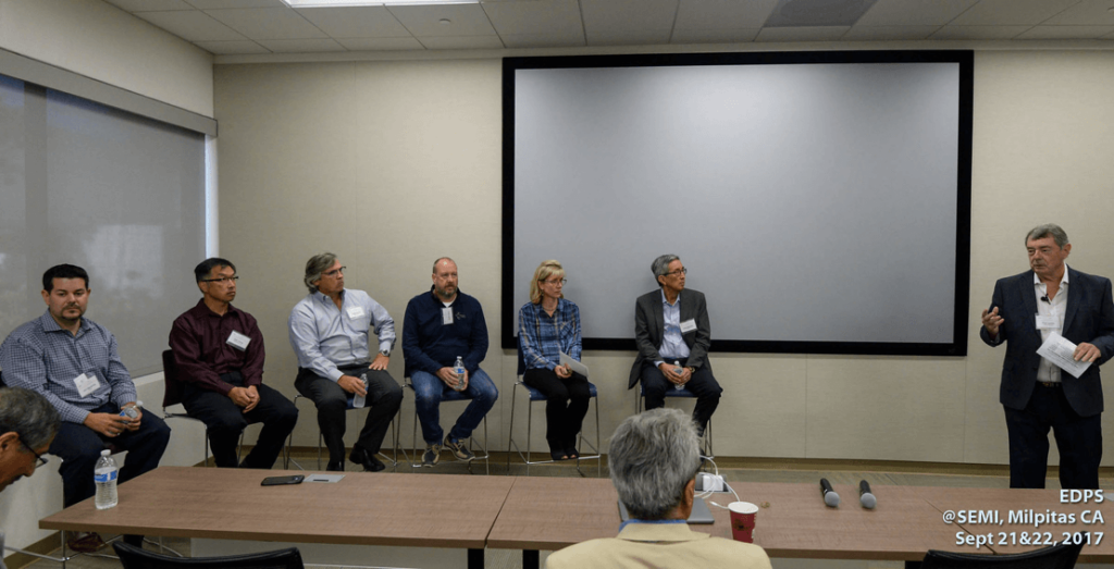
These seven people have together more than 100 years of IC manufacturing and test experience. They had high expectations because Leckie and I had promised them that we would have EDA and IC design experts in the audience to hear their requirements and concerns. We all hoped for a discussion, producing ideas how EDA tools and design methodologies, data exchange and cooperation between EDA, design, and manufacturing could be improved.
Events do not always happen as planned….
While several IC designers in the audience contributed to the discussion and agreed with the panelist’s statements, we could not engage a single EDA expert in this discussion. I promised panelists and audience to work harder to win EDA/test experts for next year’s EDPS. I hope that our industry’s EDA/test experts will start dialogs with these panelists to address test-related challenges jointly, share the rewards and present a lot of progress at EDPS in Fall 2018.
Quick EDPS summary: The 70+ attendees gave us a lot of positive feedback for this year’s conference. They got updates on challenges and opportunities, learned about new topics – like ML, got a USB stick with all EDPS presentations, and won new friends.
If you want to study a specific topic presented at EDPS or get access to all the slides, please go to The EDPS website and download pdf copies. They’ll give you much more technical depth and detailed information about the topics presented at EDPS 2017 than a brief blog can convey.
If you want to engage with the panelists in the picture above and hear what they need from EDA vendors, please contact them directly. If you need me to introduce you, email me at herb@eda2asic.com .
Please join us at next year’s EDPS. Check back here in Spring 2018 for details. ~ Herb


