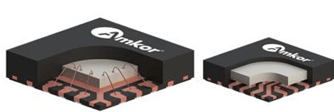
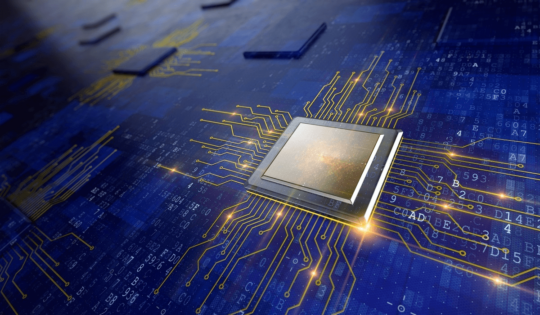
Luke Hoefer, KyungSu KimAmkor Technology Inc.2045 E. Innovation CircleTempe, AZ 85249 USA AbstractThe demand for cost-effective leadframe packages continues to...
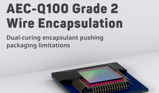
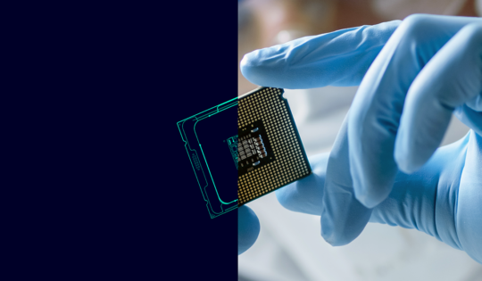
PFAS-free solution meeting stringent quality standards for automotive vision systems Modern vehicles rely on sophisticated camera systems to ensure safety...
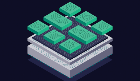
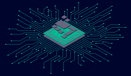
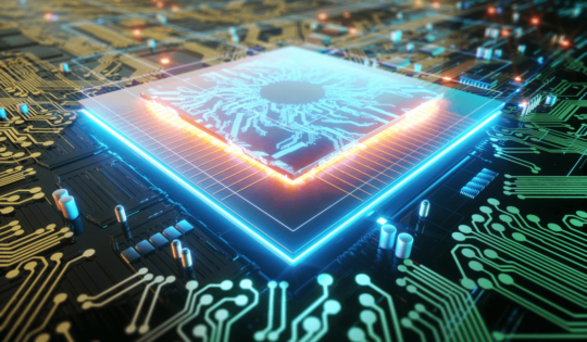
Semiconductors are the micro-sized “brains” that power modern electronics, and the latest advancements in semiconductor packaging materials are transforming key...
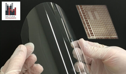
Numerous package designers possess extensive hands-on experience in crafting organic FR4/HDI build-up BGA/LGA substrates. They have mastered the design guidelines,...
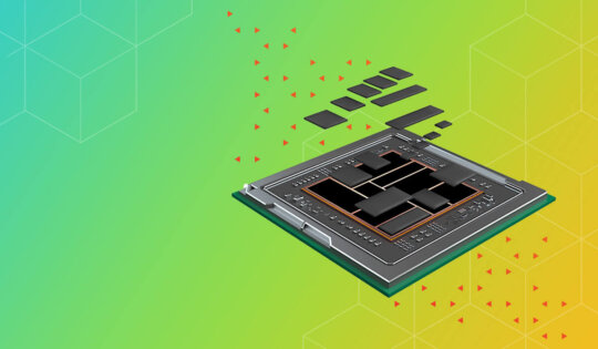
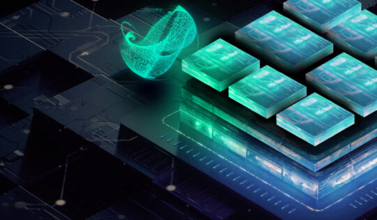
NCP and NCF Property Optimization Delivers High-Reliability Results Semiconductor package sizes are getting smaller and bump pitches narrower while the...