A number of factors are converging and driving the chiplet design revolution. To start with the economic advantage of silicon scaling is slowing.
 The semiconductor industry is facing an inflection point as higher cost, lower yield, and reticle size limitations drive the need for viable alternatives to traditional monolithic solutions, which have hit the limits of physics. A lot of these inflection point issues have been driven by a reduction in the performance and power benefits one can achieve by scaling below 10 nm, along with the expanding number of physics-related issues at the most advanced nodes, such as multiple types of noise, thermal effects, and electromigration.
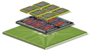
This is driving an emerging trend to disaggregate what typically would be implemented as an SoC into solid, fabricated IP blocks, or chiplets, that typically include just a couple of functions, resulting in a multi-die heterogeneous integrated implementation.
For example, HPC, AI, and other extreme data processors reach or exceed reticle sizes when using a monolithic approach. So companies such as Intel, AMD, and Marvell already utilize a chiplet design approach. Many of these are homogeneous approaches where what would have been a monolithic implementation is partitioned into multiple blocks interconnected with proprietary interfaces. However, there are efforts underway to standardize chiplet interfaces, opening the way to third-party chiplets.
Adopting heterogeneous and homogeneous integration offers a path to enhanced device functionality, faster time to market, and silicon yield resiliency. Multiple integration technology platforms have emerged that allow for cost, size, performance, and power optimizations that satisfy the need of multiple markets; such as mobile computing, automotive, HPC, AR/VR, AI, IoT, medical, aerospace, and 5G. Multiple integration technology is supported by approaches such as fan-out wafer-level packaging (FOWLP), which rose to popularity with Apple and TSMC, and with TSMC’s Integrated Fan-Out (InFO) technology. FOWLP was originally developed as a low-cost alternative to 2.5D and 3D-IC, but increased density, pillars, high-bandwidth memory, and faster interconnects have made FOWLP much more Introduction attractive to other market segments as well. Thus, 2.5D and 3D-ICs are becoming the platforms of choice at the high end of the performance/bandwidth market.

The supply chain is also gearing up to support and technology offerings, with all the major foundries supporting advanced packaging. TSMC, UMC, Global Foundries, Samsung, and others now offer sophisticated advanced packaging options. Not to be left behind, the traditional OSATs have also responded to the trend with the top two, ASE and Amkor, offering robust high-volume integration platforms.
This Siemens white paper reviews five areas that have the most impact on successful implementation and design with chiplets.