SEMICON Europa 2023, co-located with productronica in Munich, Germany makes for one of the strongest single events for electronics manufacturing in Europe. Together, SEMICON Europa and productronica showcase the entire spectrum of technologies and solutions for the entire semiconductor and electronics manufacturing industries, reflecting the rapid pace of technological development in all areas. From top-notch keynotes, market trends, exhibition and networking, next week’s show is sure to provide new insight into the future of our industry, perhaps much of this information supplied by our own 3D InCites community. Below you will find our participating members and highlighted speakers.
Be sure not to miss the 3D InCites Podcast booth. Once again, 3D InCites is serving as the Official Podcast of SEMICON Europa. Francoise will be recording at Booth: B0-208. Stop by to schedule your interview. The 3D InCites Podcast provides a forum for our community members to discuss all kinds of topics that are important to running a business in the semiconductor industry, from marketing to market trends, important issues that impact our industry, and our success stories. Additionally, 3DInCites is hosting its annual Member Appreciation event at the Augustiner Stammhaus. Co-hosted by Kiterocket and the Bavarian Chips Alliance, don’t miss this casual networking opportunity to connect with the 3D InCites community and enjoy a traditional Stammtisch-type evening with good beer, food, and conversation. Limited availability, members only. RSVP asap.

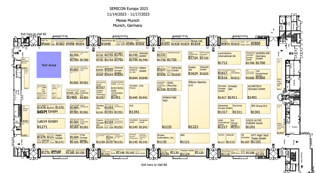
ACM Research Inc.
- Booth: B1836
ACM Research, Inc. provides advanced processing technology, systems, and key manufacturing products targeted to a range of semiconductor IC manufacturing, wafer-level packaging and SiC manufacturing applications. The company specializes in developing cleaning technologies for advanced semiconductor device manufacturing. To address increasing challenges in defect reduction that plagued emerging generations of IC chips, ACM Research developed its innovative single-wafer cleaning equipment, which features the company’s proprietary Space Alternated Phase Shift (SAPS™) and Timely Energized Bubble Oscillation (TEBO™) megasonic cleaning technologies.
ClassOne Technology
- Booth: B1441
ClassOne has become the industry’s preferred semiconductor equipment manufacturer of new, high-performance electroplating (ECD) and surface prep equipment for ≤200mm manufacturers. The company designs, builds, and delivers advanced single-wafer tools for process development and volume production, as well as batch spray solvent tools, spin rinse dryers, and more. ClassOne, works with a majority of the world’s category-leading device manufacturers, including both silicon and compound semiconductor producers of VCSELs, microLEDs, LEDs, Laser Diodes, MEMs, Power Semiconductors, RF, Photonics, IR Sensors, Microfluidics, and much more. Its equipment routinely helps fabricate devices on a broad array of substrate sizes and materials, from silicon and glass to sapphire and GaAs to InP and HgCdTe and more.
Edwards GmbH
- Booth: B1620
Edwards is a global leader of vacuum and abatement. The company is leading the industry, pushing the boundaries of science to deliver innovative products which are intrinsic to everyday life, working in partnership with its customers and continually setting new standards. Edwards is committed to reducing the negative environmental impacts of the industries served and strives to minimize their impact on the natural world and environment we live in now and for the future.
ERS Electronic GmbH
- Booth: B1736
ERS has been supplying innovative thermal test solutions to the semiconductor industry since 1970 and is famous for fast-ramping and precise low-noise thermal systems (-65°C to +400°C) for analytical, parametric and wafer sort probing up to 300mm. The patented ERS flagship product for hot/cold wafer test, AC3, is available for package-level tri-temp applications for MEMS test. ERS designs and builds stand-alone thermal-forcing systems and custom production tools for difficult thermal applications. ERS also supplies the advanced wafer level packaging market with its fully automatic debonders and warpage adjust tools used in the production of both 200mm and 300mm eWLB device packages. On a broader scale, ERS supports not only eWLB but many other Fan-Out Wafer- and Panel-Level Packaging (FOWLP & FOPLP) technologies.
EV Group (EVG)
- Booth: B1213
EV Group (EVG) is a leading supplier of high-volume production equipment and process solutions for the manufacture of semiconductors, MEMS, compound semiconductors, power devices and nanotechnology devices. A recognized market and technology leader in wafer-level bonding and lithography for advanced packaging and nanotechnology, EVG’s key products include wafer bonding, thin-wafer processing and lithography/nanoimprint lithography (NIL) equipment, photoresist coaters, as well as cleaning and inspection/metrology systems. With state-of-the-art application labs and cleanrooms at its headquarters in Austria, as well as in North America and Asia, EVG is focused on delivering superior process expertise to its global R&D and production customer and partner base – from the initial development through to the final integration at the customer’s site.
Evatec AG
- Booth: B1624
Home of the BAK and CLUSTERLINE® families, Evatec delivers complete thin film production solutions for advanced packaging, semiconductor, optoelectronics and photonics. Offering a range of batch, cluster and inline deposition systems according to customer throughput, process requirements and fab integration requirements, Evatec’s advanced process control (APC) technologies set new standards in process control through “in situ” capability for control of mechanical, optical and electrical properties during the deposition cycle. Its “in situ” techniques reduce process development times, enhance yields or increase tool throughput.
Finetech GmbH & Co. KG
Finetech is a leading supplier of manual and automatic die bonders for high-precision micro assembly and advanced die attach applications, helping customers bring visions to life in industries as diverse as aerospace, medical, biotech, consumer electronics, semiconductors, or at universities and research facilities around the world. The modularly expandable hardware and software of its die bonders enables application-specific machine configurations. Thanks to its “prototype-to-production” approach, R&D processes can very effortlessly be transferred from development to production for integrated, flexible and cost-efficient product development.
Fraunhofer IZM – ASSID
- Booth: B1221
The Center “All Silicon System Integration Dresden – ASSID” operates Fraunhofer IZMs leading edge, industry-compatible 200/300mm 3D wafer-level-process line with process modules for TSV formation, TSV post-processing, pre-assembly, wafer-level assembly, stack formation. ASSID is focusing on process development, material & equipment evaluation as well as R&D services for heterogeneous SiP solution.
Indium Corporation
Indium Corporation® is a premier materials refiner, smelter, manufacturer, and supplier to the global electronics, semiconductor, automotive, power electronics, and PCB assembly/SMT markets. Indium will announce the introduction of an innovative new product. Indalloy®301-LT is a novel alloy technology with the potential to revolutionize preform soldering by enabling lower processing temperatures for power module package-attach applications. Indalloy®301-LT offers consistent bondline thickness and improved strength, with enhanced thermal and mechanical reliability, while reducing energy input during the manufacturing process. Additional featured products at productronica include innovative solders and thermal interface material.
KLA
- Booth: B1341
KLA’s comprehensive portfolio of SensArray® products (booth B1345) enables in situ monitoring of process tools’ environments. With wired and wireless sensor wafers and reticles, an automation package and data analysis systems, SensArray® products provide comprehensive information for a wide range of wafer and reticle processes. Wafer process equipment manufacturers, IC manufacturers and reticle manufacturers use SensArray® data to visualize, diagnose and control process conditions
Koh Young Europe GmbH
Koh Young Technology is a leading provider of 3D inspection solutions. Established in 2002, Koh Young pioneered the market by launching the first 3D Solder Paste Inspection (SPI) system using a patented dual-projection Moiré technology. Since then, it has become the global leader in 3D measurement-based SPI and Automated Optical Inspection (AOI) equipment for the electronics industry. The MEISTER product family is a portfolio of True 3DTM Inspection Solutions for solder paste, printed bumps, and solder ball as well as small components like 0201Ms and highly reflective die. The Meister D is a perfect solution for production-speed 3D inspection for component and die inspection solution targeting die and small MLCCs using an integrated measurement tool with defect analysis software based on advanced optics and AI engines. The system inspects micro cracks, chipping, foreign material, and more.
LPKF Laser & Electronics SE
SEMICON Booth: B2154/ Productronica B2.303
LPKF Laser & Electronics is a leading supplier of laser-based solutions for the technology industry. Its laser systems are vital in the manufacturing of printed circuit boards, microchips, automotive parts, solar panels and many other components. LPKF’s patented Laser-Induced-Deep Etching (LIDE) technology enables the economical production of deep microfeatures in technical glasses. Under the brand name Vitrion, a team of dedicated engineers and researchers is offering of the latest process technology for thin glass focusing on added value for semiconductor packaging applications. The LIDE technology was the winner of the Productronica Innovation Award 2017. LPKF also provides electronic manufacturing systems for laser depaneling of PCBs, flex circuit cutting laser, as well as laser direct structuring systems for molded interconnect devices (MID) and PCB prototyping machines.
MKS Atotech
Atotech is a leading specialty chemicals technology company and a market leader in advanced electroplating solutions. Atotech delivers chemistry, equipment, software, and services for innovative technology applications through an integrated systems-and-solutions approach. Atotech solutions are used in a wide variety of end-markets, including smartphones and other consumer electronics, communications infrastructure, and computing, as well as in numerous industrial and consumer applications such as automotive, heavy machinery, and household appliances.
NAMICS Europe GmbH
For more than 70 years NAMICS has been working alongside our customers to provide reliable and innovative materials for individual needs, with a special focus on green alternatives without compromising on reliability requirements. At Productronica 2023 NAMICS is going to showcase its novel insulating film material for heat sink insulation for power electronics. With a minimal thickness, it still offers high breakdown voltage of 6kV. For sophisticated needs for die attach applications, we carry pressure assisted as well as pressureless sintering materials exceptional reliability properties.
Nordson Electronics Solutions & Nordson Test & Inspection (Exhibiting with smartTec)
smartTec offers comprehensive services and self-developed solutions with its strong partners in the field of manufacturing systems, process and soldering technology, and consumable products.
ASYMTEK Products has taken the lead for 35+ years to advance fluid dispensing, conformal coating, and jetting technologies. As part of the Nordson ELECTRONICS SOLUTIONS brand, ASYMTEK Products offers full solutions and we drive our technology to tailor systems for customers’ applications such as capillary underfill for stacked dies with through silicon vias (TSV), face-to-face stacked dies, and flux dispensing for die stacking. Other applications include fluid encapsulation, conductive pastes for die attach, and thermal interface material (TIM) for heat dissipation.
Nordson TEST & INSPECTION offers its customers a robust product portfolio, including Acoustic, Optical and Manual X-ray Inspection, Autonomous X-ray Inspection, X-ray Component Counting and Nordson X-ray Technologies. Nordson TEST & INSPECTION is uniquely positioned to serve its customers with best-in-class precision technologies, passionate sales and support teams, global reach, and unmatched consultative applications expertise.
Onto Innovation
- Booth: B1612
Onto Innovation is a leader in process control, combining global scale with an expanded portfolio of leading-edge technologies that include: Un-patterned wafer quality; 3D metrology spanning chip features from nanometer scale transistors to large die interconnects; macro defect inspection of wafers and packages; metal interconnect composition; factory analytics; and lithography for advanced semiconductor packaging. Its breadth of offerings across the entire semiconductor value chain combined with our connected thinking approach results in a unique perspective to help solve customers’ most difficult yield, device performance, quality, and reliability issues. Onto Innovation strives to optimize customers’ critical path of progress by making them smarter, faster and more efficient.

Plan Optik AG
- Booth: B1912
Plan Optik AG is the leading manufacturer of structured wafers when it comes to technology. Get to know Plan Optik’s wide range of wafers from glass, quartz and glass-silicon-compound materials. In sectors such as consumer electronics, automotive, aerospace, chemistry and pharmaceuticals these wafers are essential components for numerous applications in MEMS technology. At SEMICON Europa you should pay attention to Plan Optik’s wide range of patterned glass wafers as well as stock wafers by Plan Optik’s brand Wafer Universe. Special attention should be paid to Plan Optiks’s latest technologies VLIS (Volume Laser Induced Structuring) and ACT (Advanced Connectivity Technology). Plan Optik wafers are available to minimum tolerances with application-specific structuring and complex material combinations.
Plasma-Therm LLC
- Booth: B1760
Established in 1974, Plasma-Therm is a global manufacturer of advanced plasma processing equipment, providing etch, deposition, material modification, and plasma dicing technologies to the specialty semiconductor markets, including wireless communication, power devices, MEMS, photonics, advanced packaging, memory and storage, and R&D. Plasma-Therm’s products have been adopted globally and have earned its reputation for value, reliability, and world-class support. Sales and service locations throughout North America, Europe and Asia-Pacific meet the diverse needs of Plasma-Therm’s global customer base.
PTW Europa GmbH
- B1161
For more than 15 Years, PTW Group has been servicing legacy tool support. PTW’s history goes back to a workshop in Austria founded in 2007 who supported local semiconductor manufacturing plants with parts and upgrades. On 21 April 2015, PTW Asia LTD was established in Singapore to expand its support to all semiconductor and photonic factories worldwide. PTW Group now includes Jesse-Technologies (Hitachi CD-SEM support) and CinTai Formosa (ASM furnace & EPI support). By incorporating Cin Tai Formosa and collaborating with Helios, an Arizona-based company, the company significantly expanded its scope of action on ASM tools.
PulseForge
- Booth: B1644
PulseForge, Inc. utilizes applied energy in a precise and targeted manner to enable innovation in industrial manufacturing. Its expertise and tools empower customers to explore novel materials and manufacturing methodologies, driving dynamic and efficient production at an industrial scale. Digital Thermal Processing™ is a different approach to manufacturing; a whole new category that makes this future possible. It is a new means of delivering applied energy for earth- friendly, innovative manufacturing across a diverse group of global markets. PulseForge has already begun working with industry leading OEMs, advanced manufacturing leaders, and materials companies across multiple industries in order to lay the groundwork for an ecosystem to make this vision a reality. This creates a path to producing electronic products that are far more energy efficient; products that are significantly lighter (e.g. aerospace, automotive, wearables) and more compact than today.
Siemens AG
To help customers harness complexity in today’s environment, Siemens offers a comprehensive and integrated portfolio of software solutions for the electronics and semiconductor industries. Including Product Lifecycle Management (PLM), Electronic Design Automation (EDA), Application Lifecycle Management (ALM), Manufacturing Operations Management (MOM), Embedded Software and the Internet of Things (IoT) solutions that drive digital transformation for businesses of all sizes.
SurplusGLOBAL, Inc.
- Booth: B1264
SurplusGLOBAL is a seasoned global trader in the pre-owned equipment market, boasting over 23 years of experience in collaborating with semiconductor companies worldwide. With a vast inventory of more than 1,500 tools that cater to diverse pre-owned equipment needs, its comprehensive range of services includes as-is, where-is sales, rental, refurbishment, remarketing, and valuation. With an impressive depot space spanning approximately 59,504 m2, its temperature, and humidity-controlled facilities ensure optimal equipment storage conditions. Customers include a majority of the top 60 global companies.
Trymax Semiconductor Equipment B.V
- Booth: B1251
Trymax Semiconductor Equipment is an innovative plasma-based company designing, manufacturing and marketing state of the art equipment solutions for ashing, descum, surface preparation, light etching as well as UV photoresist curing and charge erase. With a product portfolio ranging from 100mm wafer size to 300mm and an installed base of 250+ systems, Trymax has significant market shares at foundries, IDMs, and Wafer Level packaging houses for end applications in Power Semiconductors, RF, Analog, Automotive, MEMS, LED, and CMOS. Recognized for its reliability, low cost of ownership, and performances, Trymax continuously innovates to support its customer’s needs.
Veeco GmbH
- Booth: B1640
Veeco is an innovative manufacturer of semiconductor process equipment. Its proven MOCVD, lithography, laser annealing, ion beam, and single wafer etch and clean technologies play an integral role in the fabrication and packaging of advanced semiconductor devices. With equipment designed to optimize performance, yield and cost of ownership, Veeco holds leading technology positions in the markets served. Its products and services help customers optimize the manufacture of semiconductors, memories, EUV mask blanks, VCSELs, photonics, advanced LEDs and displays, power electronics, compound semiconductors, hard disk drives, MEMS, wireless chips and more.
Yield Engineering Systems, Inc.
- Booth: B1141
YES provides surface and materials enhancement systems (thermal processing, wet processing, plasma cleaning, and coating) that enable innovation for technology leaders across a wide spectrum of markets, including advanced packaging, IoT, life sciences, AR/VR, MEMS, power, automotive and sensors.
SEMICON Europa Speaker Presentations
CEO Summit
Tuesday, November 14 | 10:00 am – 1:20 pm
| 11:40 | Sustainability through Innovation: a Superior Technology Story |
| Koen Lauwers, President Semiconductor Division, Edwards |
ITF towards NETZERO – Powered by imec
Tuesday, November 14 | 2:00 pm – 6:30 pm
| 15:05 | The Challenge to Reduce Emissions during a Period of Growth |
| Chris Jones, Environmental Solutions Business Development Manager, Edwards | |
| 16:55 | The Journey to Sustainable Design |
| Karna Nisewaner, Corporate VP, General Counsel & Corporate Secretary, Cadence |
Advanced Packaging Conference (APC)
Wednesday, November 15 | 9:00 am – 6:45 pm
| 09:30 | Bridging Front End, Packaging and Substrates to Advance the Semiconductor Roadmap |
| Oreste Donzella, Executive VP, KLA | |
| 09:50 | Opening Remarks by Session Chair |
| Roland Rettenmeier, Senior Product Marketing Manager, Evatec | |
| 15:15 | High-speed Die, Component 3D Reconstruction Solution by Multimodal Phase Shift Optics Approach |
| Axel Lindloff, Senior Process Specialist Pre-Sales, Koh Young Europe GmbH | |
| 15:35 | How to Achieve Upcoming Bump Requirements by Optimized ECD Plating Processes |
| Stefan Pieper, Global Application Manager for Semiconductor Processes, MKS/Atotech | |
| 16:40 | Opening Remarks by Session Chair |
| Tanja Braun, Program Director, Fraunhofer IZM | |
| 16:45 | TBD |
| Lihong Cao, Sr. Director, Engineering & Technical Marketing, ASE, Inc. | |
| 17:05 | Optimization of Advanced Packaging Process: Concept of Maskless Dual–Layer Lithographic Patterning |
| Ksenija Varga, Business Development Manager, EV Group |
Future of Work
Wednesday, November 15 | 2:50 pm – 5:30 pm
| 15:15 | Challenges and opportunities surrounding your Talent Pipeline |
| Dan Collins, General Manager, SPTS Division within KLA Corp | |
| 15:35 | Sustainability through Inclusion: how Surveys (Insights) + Analysis Support our Understanding of Generational Expectations |
| Christine Pelissier, General Manager, Customer Center EMEA, Edwards
|
Innovation Showcase
Friday, November 17 | 10:00 am – 1:30 pm
| 11:30 | Manufacturing next generation power devices – how temporary bonding allows wide bandgap power devices to go vertical. |
| Elisabeth Brandl, EVG | |
| 12:00 | Enabling smart manufacturing in semiconductor fabs using predictive design and process insights |
| Srividya Jayaram, Siemens Digital Industries Software |
Productronica
Ulf Oestermann, Fraunhofer IZM
Miniaturisierung von Leistungselektronik – Trends und Grenzen in der Zuverlässigkeit
15.11.2023 at 10:00 – 10:30
Innovation Forum
Modern power electronics devices benefit from new semiconductor materials, new interconnect technologies and new system architectures. These developments mean that power electronic systems can be made increasingly smaller and more compact, so that the power density per volume increases in a way that was previously unattainable. This inevitably has an impact on the stress on the system in its operating environment and on its lifetime.