
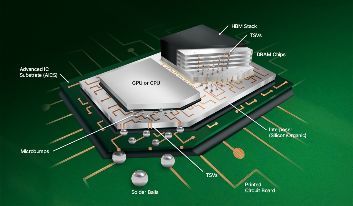
An AI package is like a puzzle made up of individual pieces of different sizes and shapes, each one essential to the final product. Together, these pieces are typically integrated into a 2.5D IC package designed to reduce footprint and maximize bandwidth.
A graphic processing unit (GPU) and multiple 3D high-bandwidth memory (HBM) stacks provide the major pieces in the AI puzzle. These puzzle pieces are first assembled on top of a silicon interposer. An advanced IC substrate (AICS) provides the foundation on which the 2.5D package is built.
While we could go on to great lengths to discuss the manufacturing of each of these AI puzzle pieces, for this article, we are focusing on the advanced packaging side of the process – the glue that holds all the pieces together – and the many manufacturing challenges of a 2.5D IC package.
But before we get into that, let’s talk about what AI is and what AI isn’t.
A Word About AI
Forget what the movies have told us. AI today has little in common with sentient machines dedicated to serving or enslaving humanity. As we know it, AI is simply a new type of technological tool. It does what other tools do: enables its users to complete tasks with more efficiency and ease. The following is a list of the different types of AI, a list that, fittingly, was created using generative AI.
Artificial Intelligence (AI): This is a broad term that encompasses all aspects of creating intelligent machines. AI is used to classify machines that mimic human intelligence and human cognitive functions like problem-solving and learning.
Generative AI: This subset of artificial intelligence uses techniques (such as deep learning) to generate new content. For example, you can use generative AI to create images, text, or audio.
Machine Learning (ML): This subset of AI focuses on prediction and classification tasks. Machine learning is AI that can automatically adapt with minimal human interference.
Deep Learning: This is a subfield of machine learning that uses artificial neural networks to mimic the learning process of the human brain. It focuses on neural networks to solve complex problems.
Each one of the above applications benefits from or needs high-performance computing capability.
Now that we have discussed AI let’s explore the packaging challenges of 2.5D AI devices further. This article will focus on the challenges associated with through-silicon vias (TSVs), microbumps, and AICS.
TSV Challenges
TSVs are a key piece of the puzzle for the construction and performance of both 2.5D and 3D packages. Designed with extremely small critical dimensions, high-aspect ratios (HAR), and fine pitches, TSVs enable high numbers of inputs/outputs and provide vertical electrical pathways for HBM and silicon interposers (Figure 1)
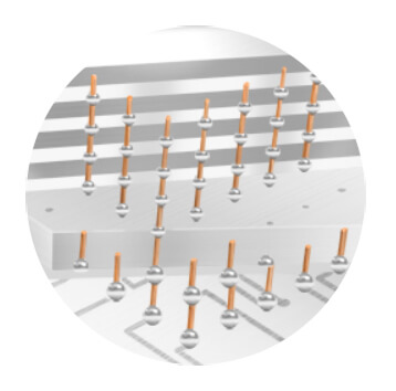
The TSV process is intensive and requires several key process steps, including etch, deposition, fill, and chemical mechanical planarization (CMP). With the demand for thinner silicon die, decreasing TSV size, and, in some cases, even higher aspect ratios, controlling the exact size and depth and finding increasingly hidden defects, is essential to maintaining high yield.
Top and bottom critical dimension (CD), sidewall profile, and depth are all important process control parameters for TSV manufacturing, as they can affect electrical performance between the stacked die. If the TSV is not etched deep enough, the two dies will not be connected even if they have been placed on top of each other. Next, the barrier/liner material is deposited with good uniformity and thickness control. Electro-plated Cu fills the TSV, where measuring the overburden thickness — as well as inspecting the Cu fill for growth defects and voids — is critical.
As for the backside of the wafer, the front of the wafer will be temporarily bonded to a carrier so the backside can be thinned to reveal the TSVs. The thinning process is important. The remaining silicon of the etched TSV must be measured and monitored for grind and blanket etch to ensure TSV interconnects are evenly revealed for stacking the chip or entire wafer. Failure to accurately measure and inspect the backside can lead to defects, distortions, electrical resistance, and device failure, which ultimately leads to increased scrap and decreased yield.
Tools that are useful to address the above challenges include metrology for advanced OCD and HAR structures and an automated high-speed sub-micron defect inspection and 2D/3D metrology system.
Microbump Challenges
in addition to TSVs, microbumps are also a key element providing the interconnections between the different components within the AI package. Besides connecting the individual DRAM layers and the logic buffer die within the HBM stack, microbumps connect the 3D memory stacks and the GPU to the interposer. Larger solder bumps also connect the interposer to the advanced IC substrate (AICS) (Figure 2.)
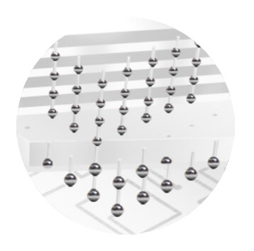
Much like TSVs, microbump technology continues to scale downward, decreasing height, diameter, and pitch. Further shrinking is expected and eventually calls for using direct Cu-Cu hybrid bonding. A primary downside of this shrinkage is maintaining plating uniformity of the bump — both within the die and across the whole wafer. This becomes more challenging. For the die to properly attach to the next component — whether it is DRAM, logic buffer die, interposer, or IC substrate — these bumps need to be the same height to ensure proper connections.
Measuring the individual thicknesses of each of the metal films used to construct the bump is also important. The choice of metal and its respective thickness are critical in controlling the performance and reliability of the device.
Another potential stumbling block with microbumps is related to defectivity: the presence of residues, cracks, voids, or to an even greater extent, where the microbump is damaged or displaced. In extreme cases, these defects result in immediate electrical shorts or failed connections. However, the impact of some of these defects may not be apparent at first but slowly evolve and affect device reliability.
Each of these challenges, if not properly addressed, will impact device performance. An opto-acoustic metrology tool using picosecond ultrasonic technology can measure both individual metal film thickness and the final total bump height. A combination of 2D/3D metrology and inspection tools can measure bump diameter and bump height, as well as detect defects, delivering in-line process control.
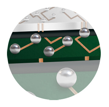
AICS Challenges
As input/output (I/O) density increases, the ability of individual components to mate directly to the printed circuit board becomes an issue. This is where AICS enters the process as a piece of the AI puzzle. AICS acts as the bridge between the package’s individual components (Figure 3). To connect the interposer above —and the die connected to it — a high number of redistribution layers (RDL) are needed. As the number of RDL layers increases, so does the possibility of overlay errors.
Speaking of RDLs, a large landing pad at the end of each interconnecting line/space (L/S) connects to the vias. The landing pad is significantly larger than the critical dimension of the RDL. This helps increase overlay tolerance. However, these large landing pads limit design space. This problem will only be exacerbated as the interconnect technology demands finer L/S. This results in the need to increase the number of RDL layers, along with an increase in cost and potential yield loss.
To mitigate this design quandary, smaller RDL landing pads are required. This can be achieved if the process overlay is improved. To accomplish this, a lithography system must analyze and compensate for distortion errors caused by the repeated thermal cycling of the copper-clad laminate (CCL) panel and dielectric throughout the buildup process. Accurate metrology data is needed to generate an optimum alignment solution. However, this data is typically available after the lithography process is completed and the overlay of the vias to the RDL landing pad is measured. It is important to analyze this overlay data and feed corrections back to the stepper to compensate for the panel distortion of future panels.
Another area of concern involves the unique nature of the AICS process. For wafer-based devices, the active circuitry construction only happens on one side of the wafer. But for AICS, both the front-side and the backside of the panel will be processed. This significantly increases the risk of yield loss from defects caused by surface contamination. In addition, AICS has relatively few packages per panel. For example, a 510mm x 515mm AICS panel can only accommodate 16 packages (120mm x 120mm) compared to fan-out panel-level packaging (FOPLP), which could have over 2,300 packages. In other words, one defective package on an AICS could result in a 6.25% yield loss, whereas with FOPLP, one defective package may represent a 0.04% yield loss. As AICS package sizes increase to 150mm x 150mm, yield challenges are exacerbated: a single defective package failure results in an 11% yield loss.
Plating, dry film resist and buildup film lamination non-uniformity, RDL line defects, and more subtle buried defects, such as under-laminate bubbles and particles, can all contribute to yield loss. More stringent process control via metrology measurements and inspection after each critical step alerts manufacturers of a potential process excursion so that immediate corrective action can be taken. AICS manufacturing is a lengthy process and takes weeks to process both sides of the panel. As such, the real-time tracking of yield at every layer can help reduce the amount of time spent on processing defective substrates.
Conclusion
Advanced packaging is just one piece of the AI puzzle, but in this More Than Moore era, the back end of the process is more important than ever. In this article, we’ve outlined several key challenges facing the advanced packaging of AI devices, from measuring CD and identifying defects related to TSVs and microbumps to the real-time tracking of detective packages in the AICS production process. With the AI market driving current semiconductor industry growth, the solutions described here will become key pieces to completing the puzzle of how to meet the rapidly surging demand for AI packages.
This article first appeared in the 2024 3D InCites Yearbook. Read the full issue.


