The semiconductor ecosystem is facing a significant workforce gap, with industry demand continuing to grow faster than the available talent pool. Long-term projections suggest the semiconductor workforce pipeline will struggle to keep pace with this growth. The National Science Foundation’s estimates indicate that between 60,000 and 100,000 semiconductor roles in the United States alone could remain unfilled by 2030 if workforce development efforts do not expand.
While cutting-edge technologies continue to shape the future of the semiconductor industry, sustaining that progress will require a steady pipeline of skilled professionals to support development, manufacturing, and implementation. As a result, workforce development has increasingly become recognized as a critical priority for the semiconductor ecosystem.
At this year’s IMAPS Device Packaging Conference (DPC) in Arizona, efforts to address this challenge were visible across multiple areas of the event. Programming designed specifically for students, including technical sessions, student research presentations, and poster exhibition displays highlighted the conference’s emphasis on cultivating future talent.
Initiatives extended further, with high school outreach programs that underscored the importance of engaging future generations earlier. Together, these efforts reflected a broader industry trend: ensuring that workforce development remains a central focus as semiconductor innovation continues to accelerate.
Professional Development and Student-Industry Session
At the start of the conference on Monday, IMAPS made this priority clear by offering 19 Professional Development Courses (PDC), that offered a wide range of deep technical dives for both students and professionals looking to expand their advanced packaging expertise.
Andy Cox, a PhD student at Arizona State University who attended several of these lectures described their value: “In a traditional classroom setting, a course unfolds over an entire semester, whereas these sessions deliver the core insight of a specialist’s expertise in under two hours.”
Cox noted that while there can sometimes be a separation between academia and industry, the PDCs helped bridge that gap by exposing students to the cutting-edge work shaping the field. Beyond providing foundational knowledge, these sessions can also spark deeper interest in specialized areas of the industry. Not able to make it to the classroom sessions? You can explore additional courses available to all on the online IMAPS Academy database.
Parallel with these courses, IMAPS hosted “Future Connect”, a student-industry session designed to help students explore the transition from classroom to career. Participants learned about the benefits of IMAPS membership while hearing directly from professionals about career pathways, continuing education opportunities, and ways to make an impact within the semiconductor ecosystem.
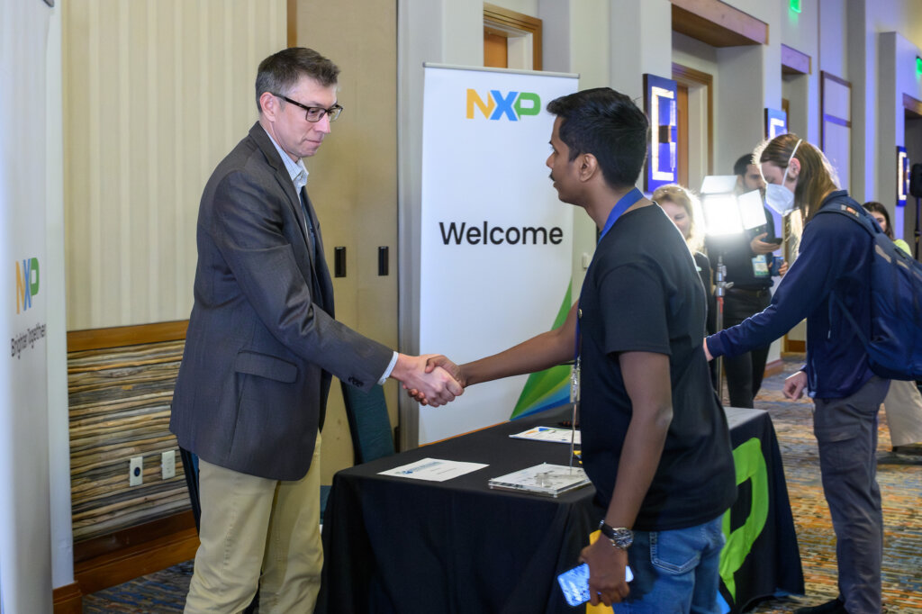
One highlight of the event was the roundtable networking session, where students were able to connect directly with industry professionals from organizations including Amkor Technology, NXP Semiconductors, Cadence, Saras Micro Devices, VIEW Micro Metrology, and Henkel. Compared with traditional career fairs, often crowded with thousands of attendees, the roundtable format created space for meaningful one-on-one conversation with experienced industry professionals.
Faith Birgen, an ASU student pursuing her master’s in Materials Engineering emphasized the value of this interaction. “Seeing my coursework through an industry lens helped me understand how the skills I’m learning in university translate into real career paths,” she explained.
These interactions demonstrated how direct engagement with industry professionals can help students seamlessly connect their academic work to real-world opportunities.
Early Pipeline Development: Hamilton High School Semiconductor Program
“Workforce development is rooted in collaboration. It takes two to tango, academia and industry, and both have played an important role in creating curriculum that align with the industry”, Scott Hayes, Director of IMAPS explained when discussing the partnership between IMAPS and universities, a collaboration that is now beginning to extend even further into high school level education.
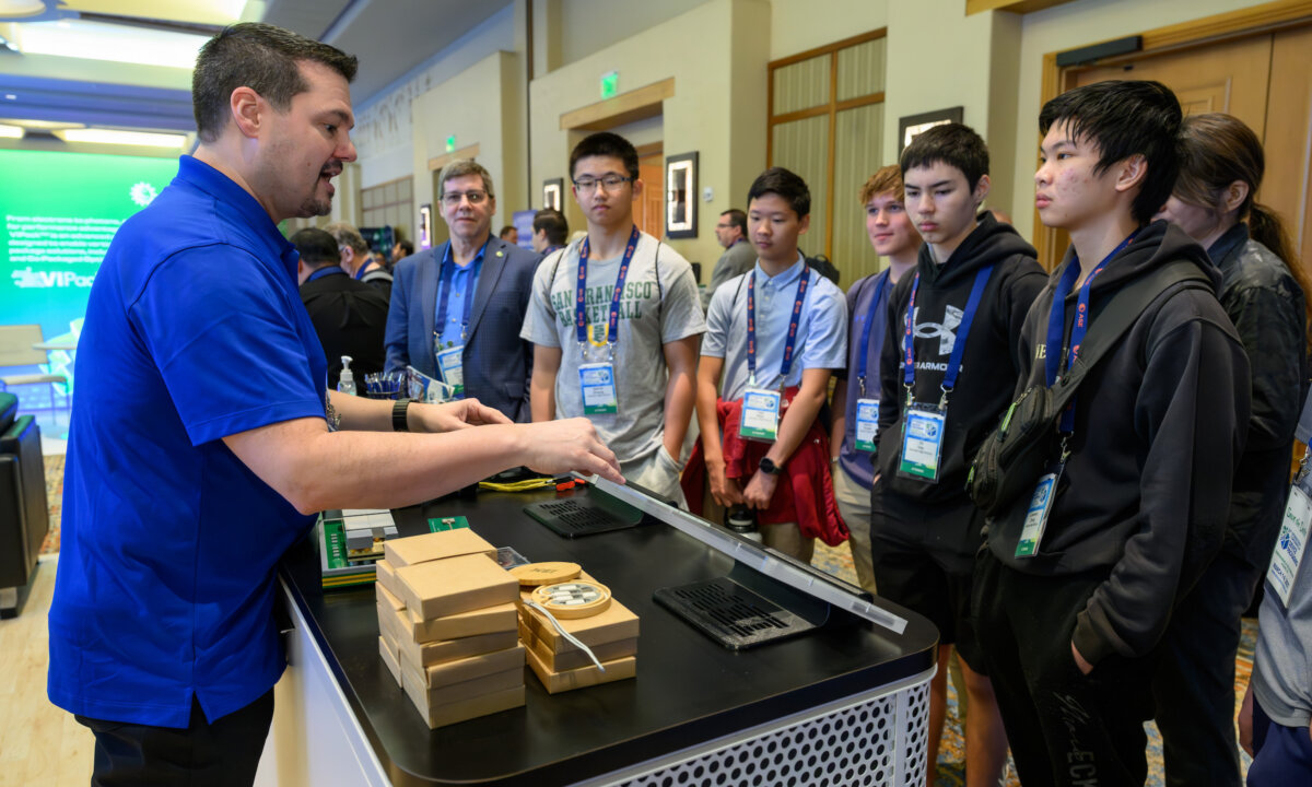
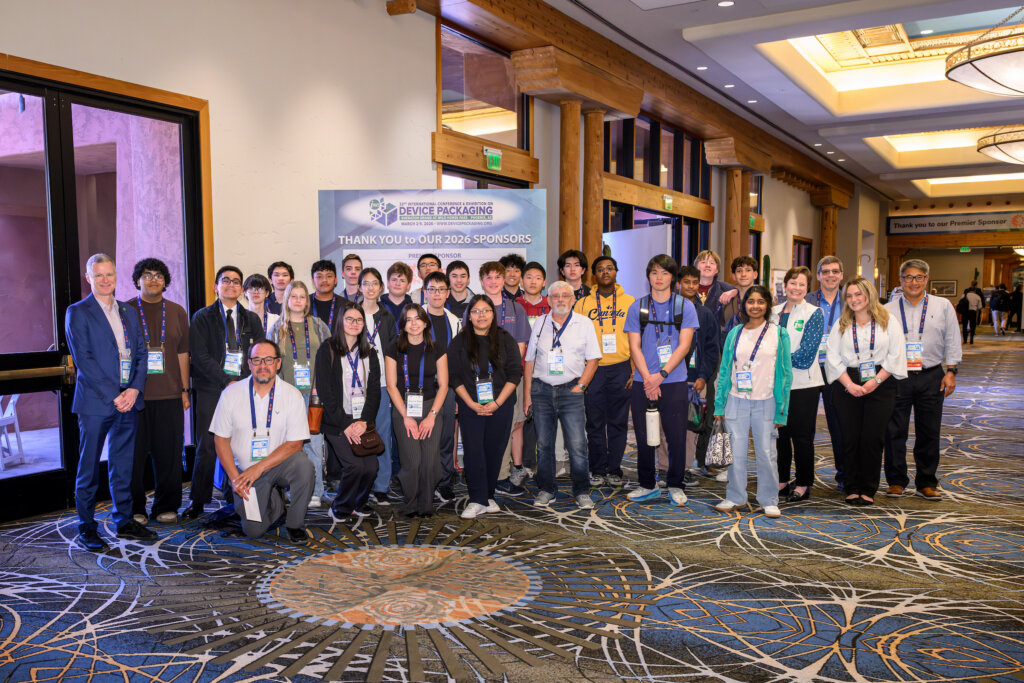
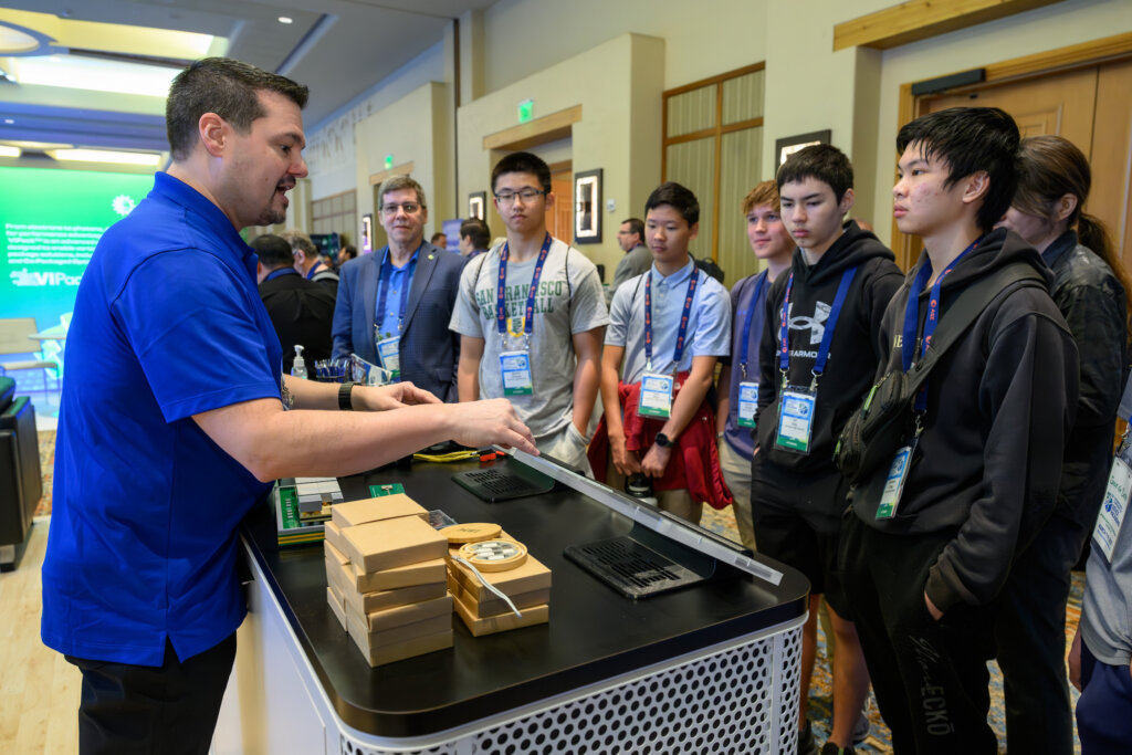
A unique and exciting aspect of this year’s DPC was the presence of students from Hamilton high School—the first high school in the United States to offer a semiconductor-focused program.
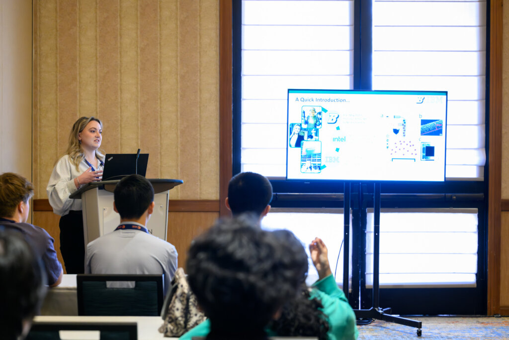
The students were welcomed with a variety of giveaways before hearing from Emma Pawliczak of IBM and IMAPS executives, who introduced the fundamentals of semiconductors and discussed the next step for building an educational foundation in the industry.
Afterward, students were able to walk through the exhibition hall, learning about the nuances of each stage of the semiconductor value chain from company representatives across the ecosystem.
By welcoming these students to experience the conference firsthand, IMAPS highlighted the growing effort to introduce semiconductor education earlier in the academic pipeline and inspire the next generation of industry professionals. The students were engaged, curious, receptive, and very excited to be there.
Empowering Students: New Travel Grant and Scholarship

In addition to hosting these student-specific events, students were also given the opportunity to present and teach professionals their own research.
I had the opportunity to attend various PhD student-delivered presentations from a wide range of universities including Arizona State, Texas A&M, University of Texas at El Paso, Georgia Tech, Auburn, Purdue, North Texas, and more.
Students were given the platform to share their breakthroughs and research, and be active, participating as members of the society. IMAPS continues to lower barriers for emerging talent, offering FREE student membership and chapter opportunities for post-secondary students and discounted rates for early-career professionals.
IMAPS intends these contributions to be the first of many commitments to workforce development. In addition to programming aimed at students, the organization also announced a new initiative designed to reduce one of the most common barriers to student participation in industry conferences: travel costs.
The newly introduced student travel grant will provide financial support to help students attend IMAPS events such as the Device Packaging Conference and the annual IMAPS Symposium.
As Scott Hayes explained, the goal is clear: “The student travel grant is intended to get students to the conference themselves.” While many students are eager to participate in conferences, travel expenses can often be a limiting factor and the gap for students to get onsite. “We want to close that gap. IMAPS is interested in making sure that the next generation of microelectronics professionals has a pathway into our industry,” said Hayes.
Those interested in receiving the travel grant will apply through the conference’s existing technical submission process. Students who submit an abstract for the IMAPS Symposium or Device Packaging Conference will have the option to opt-in for consideration during submission.
Available to both undergraduates and graduate students, applicants must be enrolled in a microelectronics-related academic program, and their submissions will be evaluated by the IMAPS Foundation’s Board of Trustees. Selected recipients will receive a $2,000 travel grant to help offset transportation and participation costs. All student members also receive a reduced registration rate for all IMAPS events.
By tying the grant directly to the abstract submission process, IMAPS hopes to encourage greater student involvement in the technical program while ensuring that emerging researchers can share their work with the broader microelectronics community.
Alongside the travel grant, the IMAPS Microelectronics Foundation also continues to support students through the educational 3D InCites Scholarship Fund unveiled at DPC. As Hayes explained, the scholarship is designed to address another aspect of workforce development by helping students offset the broader costs of higher education.
Funded through donations raised by the 3D InCites community, the scholarship provides meaningful financial support to students pursuing microelectronics-related schooling. The award is intentionally designed to make a tangible impact, offering $10,000 annually to help cover expenses such as tuition, books, and other costs related to academia.
A unique aspect of the 3D InCites Scholarship is that each awardee is also paired with an IMAPS industry mentor. “This liaison provides career guidance and networking support, helping students get integrated into the industry while building professional connections that can be critical for launching their career,” said Hayes.
On top of that, the fund aims to support underrepresented groups in the microelectronics industry, with a specific focus on expanding opportunities for women entering the field.
Conferences, further education, and mentorship often serve as a gateway for students to connect with more experts, present research, and begin developing the relationships that lead to careers in the field. As Hayes noted, long-term success of both the travel grant and scholarship would mean seeing these students return to conferences later in their careers, “growing from being a student to an industry professional and continuing the pipeline.”
Continued support from industry partners and community members will be essential to sustaining programs like this. By contributing to initiatives that help students participate in the technical community, the development of the next generation of microelectronics professionals is directly being fed.
Learn more about how you can contribute to the future of the microelectronics workforce.