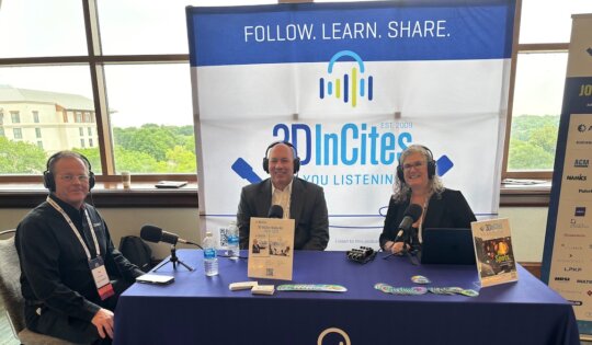
How to start what is potentially my final blog for 3D InCites: Memories, So Long, Farewell, (that one might get me in trouble), or Back to the Future? I started this venture at SEMICON West in 2019, where I helped Françoise cover the show and wrote my first 3D InCites...
As Benjimen Franklin said, shortly after the US Constitution was written, “In this world, nothing can be said to be certain, except death and taxes.” I’ll add one comment to that: Change. Change is constant. Over the past year, there has been a significant amount of change in the semiconductor...
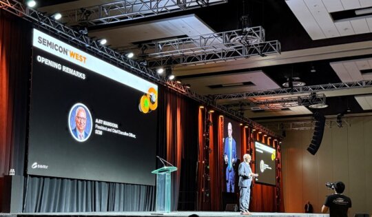
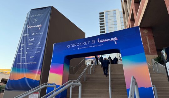
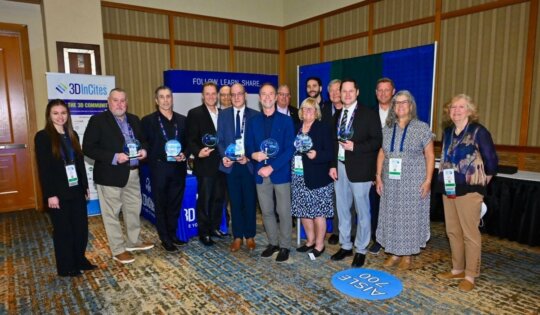
In the past 16 years, 3D InCites has watched the 3D packaging industry grow. The philosophy of 3D InCites was to create an advanced packaging community. At SEMICON West in Phoenix, the community was out in force, from ribbon-cutting ceremonies for new facilities, to new packaging equipment companies showing for...
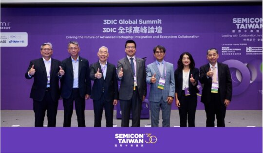
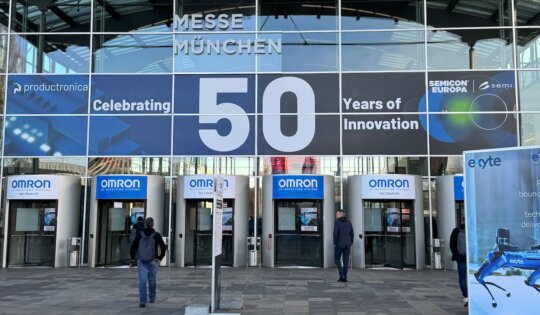
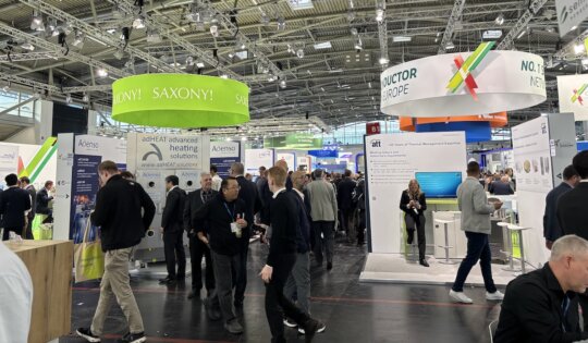
This Fall has been a busy time for semiconductor events. Starting with SEMICON Taiwan at the start of the month, IMAPS in Late September into early October, followed closely by SEMICON West last week. Fortunately, there is a month off to catch your breath before heading to Semicon Europa. There...
While raising my daughters, I ascribed to the philosophy: “A parent’s charge – give them roots and give them wings.” I believe this also applies to brainchildren. At some point, your work is done, and rather than clinging to them and holding them back, you let them go, so they...
While announcing my retirement after 20 years in the industry at IMAPS Symposium brought my career in advanced packaging full circle, wrapping up my 3D InCites career at SEMICON Europa brought closure. It was at SEMICON Europa 2007, held in Stuttgart, where my fascination with 3D integration and packaging first...
Maybe it’s my impending retirement, but I’m feeling a little salty these days. This my fifth draft about the highlights, low-lights and Aha moments of both IMAPS Symposium and SEMICON West. And I can’t get it right. All that comes up is my annoyance with carefully crafted messaging because nobody...
I recently realized that IMAPS Symposium 2025 marks my 20th anniversary in the microelectronics industry. It was the first industry event I attended, as the Associate Editor of Advanced Packaging Magazine. My first SEMICON West was in 2006, and my first SEMICON Europa was in 2007. That was when I was first...
The International Microelectronics Assembly and Packaging Society (IMAPS) is pleased to announce a major milestone for the Society, with IMAPS taking over the “stewardship” of the trusted 3D InCites platform which was owned by Françoise von Trapp and her partner Martijn Pierik. Following Françoise’s retirement, IMAPS purchased the 3D InCites...
Before a chip becomes a CPU or GPU, it undergoes a complex journey through fabrication, assembly, testing, and packaging, often spanning continents. With major OSAT facilities still offshore, the packaging process adds cost, delays, and emissions, while every hand-off increases the risk. For businesses managing key semiconductor materials and components...
December 2025 was an action-packed month for the 3D InCites community and the semiconductor industry. Major leadership appointments, innovative technology launches, and global collaborations highlighted the month. Advances ranged from AI-powered process optimization and hybrid bonding production to new materials and solder solutions. Industry events showcased cutting-edge manufacturing experiences and...
It’s bittersweet to be writing my last blog post for 3D InCites after 50+posts over four and a half years. My professional relationship with Francoise goes back much further to when we were both at Advanced Packaging Magazine 20 years ago. In Dec of 2015, Francoise approached me about writing...

Since 2009, when Francoise started 3D InCites, she’s been sharing her insights on advanced packaging – an industry, she told me, that people used to dismiss. “Back then, advanced packaging was still seen as a cost-adder, versus adding value through enhanced performance.” she said. So much has changed since then....
I recently attended SEMICON Europa in Germany to learn how the EU is approaching the next phase of its semiconductor development. From what I learned, the EU is moving its industry forward by planning for its CHIPS Act 2.0 legislation, attracting new investments, and funding competitive R&D pilot programs. In...
Co-packaged optics is one of the most talked about innovations in advanced packaging right now, and it’s for good reason. It promises higher bandwidth density, lower power consumption, and reduced latency over other packaging approaches – all of which are essential for enabling smarter AI solutions. To learn more about...
Last year, I wrote a blog on the growth of AI, where I broke down the public hype around the technology and the barriers preventing it from scaling further. Earlier this year, Gartner projected that worldwide AI spending will reach $1.5 trillion by the end of 2025, up $490 billion...
By now you know that Francoise von Trapp is retiring from 3D InCites. That has led me to also pull the curtain down on “Insights from the Leading Edge” or IFTLE as it has become known. As I told you all in IFTLE 500, IFTLE’s predecessor PFTLE (Perspectives from the...
Amkor and Intel report that they are teaming up for Amkor high volume manufacturing (HVM) of EMIB due to “interest from the AI Industry.” Through this agreement, Amkor will implement EMIB assembly processes at its Korea, Portugal and upcoming Arizona manufacturing facilities, creating an alternative source for this advanced packaging...
SEMI Investment Act Tax Credit to Include Materials Suppliers SEMI, the industry association, has announced support for the introduction of the Strengthening Essential Manufacturing and Industrial Investment Act (the SEMI Investment Act) which would extend the Advanced Manufacturing Investment Tax Credit established under the U.S. CHIPS and Science Act through...
Adeia vs AMD Hybrid bonding is a semiconductor packaging technique that enables direct Cu-Cu and oxide-to-oxide connections, eliminating the connection using microbumps. This approach improves interconnect density, electrical performance, and thermal efficiency, making it an important advanced packaging technology for next-generation semiconductor devices. Adeia Semiconductor Solutions, a wholly owned subsidiary...
November was a dynamic month for the 3D InCites community and the broader semiconductor industry, with companies showcasing innovative technologies, celebrating...

In 2024, electronics cargo theft, including semiconductors, servers, and high-end computing equipment, surged dramatically, exposing a critical vulnerability in supply...
The recent IMAPS Onshoring workshop included Scott Sikorski, IBM Global Business Development Leader, reviewing details of their onshore advanced packaging...
At the recent IMAPS Onshoring Workshop, Greg Kleese, Director of Aero & Defense Business Development, GlobalFoundries, made the presentation “GlobalFoundries...
The month of September saw continued momentum in the semiconductor industry, highlighted by exciting industry events, innovative technology launches, and...
Plus: TSMC Packaging in AZ; Deca/Microchip/SST Non-volatile Memory Packaging Taiwans Minister of Economic Affairs reports that he received information about...