

Below the Surface: From Substrate to System—Why Integration Is the Real RF Breakthrough
By Chandra Gupta In my last column, I described the ceramic substrate itself, and why material choice matters so deeply in RF, microwave, and millimeter-wave applications. Dielectric constant, loss tangent, thermal conductivity, stability across temperature, and frequency are the physical rules that govern whether a signal arrives intact or collapses...
Advanced Optical Metrology for Wire Bond Inspection Using 3D Area Multi-Focus (AMF) Imaging
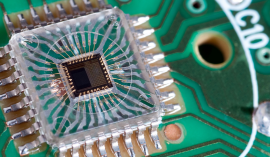
By Austin Rose, Troy Frappier and Alan Emmans of VIEW Micro Metrology Abstract Wire bonding remains one of the most widely used semiconductor interconnect technologies, supporting applications ranging from power electronics and automotive devices to memory packages and legacy logic. Shrinking wire diameters, combined with material variability across aluminum and...
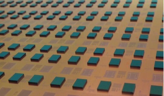
Expanding the Chiplet Market: Processing Any Wafer from Any Foundry
In response to the rising costs of advanced nodes and the slowdown of Moore’s Law, major vendors – AMD, Intel, Apple, and Samsung – are making the shift towards chiplet-based systems using 3D technologies, which create novel system partitioning through modular and scalable architectures. These solutions optimize bandwidth with respect...

Autonomous Vehicles Drive AI Advances for Edge Computing
Advances in Edge Computing Must Innovate for Autonomous Vehicles to Realize Their Potential Large numbers of sensors, massive amounts of data, ever-increasing computing power, real-time operation, and security concerns required for autonomous vehicles are driving the core of computation from the cloud to the edge of the network. Autonomous vehicles...
48V Ecosystem and Power Packaging Trends
With each passing year, emerging growth application areas such as Automotive, Cloud Computing, Industrial Automation, and Telecom (5G) Infrastructure are garnering more attention. Although the application segments are different, there is a commonality in how voltage conversion and power distribution are achieved at the system level. System demands are becoming...

Artificial Intelligence: A New Era of the Advanced Packaging Industry
Artificial Intelligence (AI) is driving the development of 3D TSV and heterogeneous integration technologies. With its new 3D TSV & 2.5D business update report, Yole Développement (Yole), part of Yole Group of Companies investigates the advanced packaging industry and takes a closer look at the AI impact on this market....

The Future of Image Sensors is Chip Stacking
CMOS image sensors (CIS) have often been heralded as the first 3D devices in volume manufacturing. However, this is not really the case. Shellcase MVP, the first generation of CIS that used through silicon vias (TSVs) to form interconnects was still a 2D device. (Remember, TSV is not always synonymous with 3D)....
3D App Update
Because someday soon, we will find more 3D TSV devices than just CMOS image sensors inside mobile applications, I like to keep my eyes and ears open for what’s going on in those areas. Here are a few interesting tidbits I came across lately. Forget what you heard about TSMC...
This Week in 3D IC News (Oct 8-12)
All Programmable PlanetToday All Programmable Planet’s newsletter appeared in my inbox, with a great post by Max Maxfield on the Xilinx family of 3D FPGAs. Beyond the detailed descriptions of Xilinx’ products, and explanation between the difference between 3D FPGA and 3D Heterogeneous FPGA, I especially like Max’s musings on...
Important stuff – but first, some 3D Friday fun
Fridays just kind of creep up on you, don’t they? It’s been a busy week in the 3D blogosphere – and not just on 3D Incites. I’m a little disappointed that nobody wanted to play the “how do you use your mobile device” game I started on Monday with these...
EV Group’s GEMINI Wafer Bonding System First to Pass Equipment Maturity Assessment within SEMATECH’s Interconnect and Manufacturability Program
SEMICON West, San Francisco, Calif., July 10, 2012 — EV Group (EVG), a leading supplier of wafer bonding and lithography equipment for the MEMS, nanotechnology and semiconductor markets, today announced that its GEMINI® Automated Wafer Bonding System has become the first product to pass a systematic, rigorous Equipment Maturity Assessment...
3D in the iPhone 5 and Other Teardown Discoveries
“It’s just like peeling a banana” reads the caption on one teardown photo describing the careful dissection of the iPhone 5. . But if you really want to see how it was done, check out this initial teardown video produced by iFixit. It’s been 3 days since Chipworks tweeted anything...
Apple iPhone 5 Teardown; More on FinFets; Thoughts on 3D Test; (and some Friday Fun at the End)
Somehow the social media “shares” on Friday are more lighthearted than the rest of the week. Today, all the excitement was divided up between the iPhone 5 teardown and the last flight of the spaceshuttle Endeavor, as it toured its way up the California coastline riding piggyback on a 747....
When 3D is 3D IC, and When it’s Not
Some of the best news to read (especially on a Friday) is non-news, like this report by Ann Steffora Mutschler, in SemiMD on how 3D ICs will not impact computational lithography tools. According to her sources, this particularly true with regards to TSVs, because of their large size in comparison...
Ziptronix Takes on 3D Memory
After seeing the latest press release on Ziptronix foray into the memory space, I sought out Kathy Cook, business development manager at Ziptronix, at ECTC to get the full story. We’ve been reading and hearing a lot about Ziptronix ZiBond process being used in CMOS image sensor (BSI) technology, and particularly...
Glass vs. Silicon Interposers for 2.5D and 3D IC Applications
There has been enough interest stirred up in R&D around glass as a low-cost alternative interposer substrate material compared with silicon, that there was an entire session dedicated to developments in that area at the 2012 IMAPS International Device Packaging conference, held March 5-8 in Scottsdale, AZ. Rao Tummala, of...
Perspectives on 3D Integration: The Researchers
To listen to John Lau, of ITRI, speak on the topic of 3D integration is to experience a passion for technology that rivals no other; except perhaps that of Rao Tummala of Georgia Tech. But John is definitely more vocal in his passion. Rao has a softer, gentler approach. At...
IMEC Tech Forum Looks at Smartphones Today and in the Future
In this brave new world powered by consumer electronic devices that cater to the user experience, smartphones and tablets are in the driver’s seat; pushing researchers to the very limits of possibility. At imec’s technology form on Smartphones, held for the first time during SEMICON West, researchers from the institute...
Thermocompression Bonding for Microbump Flip Chip Soldering
An excerpt from the Semiconductor Assembly Blog by Andy C. Mackie, Global Product Manager for Indium Corporation's Semiconductor and Advanced Assembly Materials. For reasons that I will discuss in a post later this year, a common factor that is emerging in the area of copper-pillar microbump 2.5D and 3D joining,...
3D: You’ve Come a Long Way Baby!
This column by Francoise von Trapp appeared in the Jan/Feb 2011 issue of Chip Scale Review It sums up a lot of what was said at various 3D IC events over the past few months. A year ago, there were still skeptics in the room at the annual 3D Architectures...