
To listen to John Lau, of ITRI, speak on the topic of 3D integration is to experience a passion for technology that rivals no other; except perhaps that of Rao Tummala of Georgia Tech. But John is definitely more vocal in his passion. Rao has a softer, gentler approach. At this year’s IWLPC in Santa Clara, both expressed their perspectives on what they see as the most cost effective and immediately available path to achieving 3D integration using passive TSV interposers as either substrates or carriers.
In an almost 2 hour impassioned presentation, Lau gave a history and future lesson of 3D integration. He talked about the William Shockley, the co-inventor of the transistor, and as it happens, the through silicon via (TSV). Except Shockley didn’t call it a TSV and it wasn’t intended for 3D IC integration. In those days, the original via holes were used for grounding. That was 50 years ago.
Lau also talked briefly about 3D Si integration, which he defined as a bumpless, solderless, process suitable for fab manufacturing, but still a good 8 years from adoption due to cost and issues to be ironed out. Yet Lau is firmly behind 3D silicon as the ultimate solution. “3D SI is the right way to go and the right way to compete with Moore’s law,” he said.
1965 Nobel Physics laureate, Richard Feynman, lectured in Tokyo in 1986 on the topic of 3D silicon integration. “He not only told us to go for 3D, he showed us how to do it!” noted Lau.
Subsequently, Japan established a 3D roadmap in 1986, with plans for 3D Si to be designed and realized in a chip between 1990 and 2000. MIT developed 3D SI integration using face-to-face bonding of wafers with vias etched through the deposited buried oxide layer. He said Leti, Freescale and ST Microelectronics were all working on 3D Si integration bonding via –first, SiO2 wafers. In these, the TSV diameter is <1µm and PVD tungsten filled.
The technology has existed – so what happened? “As with all disruptive and emerging technologies, the question is what is it displacing? What is the cost?” noted Lau. “Nothing will be done until there is no other way to do it.” And there is still the matter of thermal management to be worked out, because without bumps, there’s no way to get the heat out. Still, Lau says the industry “should STRIKE to make this happen!”
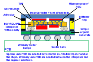
In the mean time, he says 3D integration can be realized through the use of passive interposer technology, with TSVs through passive silicon die rather than the active die, and using these interposers as either substrates with active die mounted on one side in a 2.5D configuration, or as a carrier with active die mounted on both sides of the passive interposer. The passive interposer becomes the most effective 3D IC integrator!” say Lau “It could be very low cost because we don’t have to dig and fill the holes on the active devices dies. Also, we don’t have to thin and metalize the active dies. Furthermore, we don’t have to temporary bonding and de-bonding of a supporting wafer to the active devices wafers. Let the passive interposer be the workhorse of our 3D IC integration SiP before the 3D Si integration time comes!”

3D the Georgia Tech Way
During his brief presentation and throughout the panel discussion that took place later in the day, Tummala both echoed Lau’s sentiments while also putting the Georgia Tech spin on it. At the 3D Packaging Research Center at Georgia Tech, Tummala and his team have established an industry/academia consortium to develop 3D interposer technologies using silicon or glass as the interposer substrate. Tummala reports that he’s got 27 companies involved in this industry-funded program for technology development including manufacturing suppliers for materials, tools and process as well as end users such as Qualcomm, ST Microelectronics and Maxim.
Tummala cited the benefits of the 3D passive interposer technology. He said the processes don’t disrupt the wafer fab, and no real estate is sacrificed due to TSV placement in active areas. Additionally, the process is scalabable, testable, is low cost, and has minimal thermal issues. The one stumbling block is a low cost solution for what he calls “through package via (TPV)”. He said they have developed a process in which all the vias are fabricated at one time through the glass interposer.
Another benefit of passive TSV interposers in both 2.5 and 3D configurations is the flexibility for heterogeneous integration. The ultimate 3D system may indeed incorporate MEMS, ICS, Logic, and what have you all connected thanks to a 3D TSV interposer.
Conclusion
If cost is king, and the idea is to minimize disruption through the supply chain, Both Tummala and Lau could be spot-on with their push for 3D passive interposer technology, at least until 3D Si integration is ready for prime time. – F.v.T.


