
By Austin Rose, Troy Frappier and Alan Emmans of VIEW Micro Metrology
Abstract
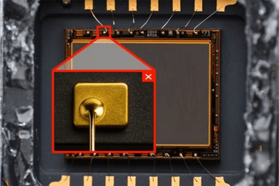
Wire bonding remains one of the most widely used semiconductor interconnect technologies, supporting applications ranging from power electronics and automotive devices to memory packages and legacy logic. Shrinking wire diameters, combined with material variability across aluminum and copper to gold and palladium coated alloys, have increased inspection complexity, particularly for measuring wire loop geometry, electrical continuity, and bond placement on highly-reflective surfaces. Conventional optical inspection systems often struggle to resolve the tops of shiny wire loops, accurately capture Z-height data, or reliably detect fine-pitch interconnect defects.
This paper examines an advanced wire bond inspection approach using an optical dimensional metrology system equipped with three-dimensional (3D) Area Multi-Focus (AMF) imaging, multiple illumination modes, and flexible software-driven 3D measurement capabilities. A representative wire-bonded semiconductor device is used to demonstrate evaluation of loop height, wire continuity, pad and lead placement, and wire-to-wire interactions. Results show that high-quality optics, configurable multi-angle illumination, and AMF-based 3D measurement enable reliable, traceable characterization of complex wire bond geometries, overcoming key limitations of conventional optical inspection methods.
An Enduring Interconnect Meets Rising Inspection Demands
Despite rapid adoption of flip-chip, wafer-level, and hybrid bonding technologies in advanced logic and artificial intelligence devices, wire bonding continues to account for a substantial share of the semiconductor packaging market. Industry projections estimate the wire bonding market will reach approximately USD 8 billion by 2035, driven by continued growth in electric vehicles (EVs), power electronics, Internet of Things (IoT) devices, and other high-reliability applications. In these segments, wire bonding remains a compelling solution due to its cost efficiency, process maturity, and adaptability across a wide range of package architectures.
At the same time, wire bond inspection requirements have become increasingly complex. Beyond verifying bond presence, manufacturers must evaluate loop geometry, electrical continuity, bond placement accuracy, and spacing between adjacent wires. These challenges are compounded by the transition to ultra-fine wire diameters, now approaching eight microns and below, and the widespread use of highly reflective metals such as gold, copper, and aluminum. As a result, many conventional automated optical inspection and vision systems lack the depth resolution, contrast control, and configurability required to reliably inspect these features.
Materials and Design Trends Complicating Wire Bond Inspection
The industry’s shift from gold wire to copper and palladium-coated copper has introduced optical inspection challenges. While copper offers cost and electrical performance advantages, its surface characteristics and reflectivity often reduce image contrast in traditional imaging systems. In parallel, wire loop profiles vary widely with package architecture, die stacking strategies, and thermomechanical requirements, limiting the effectiveness of fixed or two-dimensional (2D) inspection methods.
As device footprints shrink, smaller wire diameters and tighter pad pitch place greater demands on optical resolution and measurement repeatability. Resolving adjacent wires, detecting wire sag or deformation, and verifying loop height become increasingly difficult using 2D imaging alone. Consequently, many inspection systems struggle to reliably capture the tops of reflective wire loops, accurately measure Z-height and loop geometry, maintain consistency across wire materials, and provide traceable quantitative dimensional data rather than simple pass/fail results. These limitations raise the risk of yield loss, reliability issues, and latent field failures, particularly in demanding automotive and aerospace applications.
Advanced Optical Metrology for Robust Wire Bond Evaluation
The wire bond inspection approach evaluated in this study uses a precision optical dimensional metrology system designed for both production and laboratory environments. The system combines high-resolution imaging, flexible illumination control, and software-driven 3D measurement to address the challenges of modern wire bond inspection.
Imaging is performed using high-quality apochromatic microscope objectives spanning magnifications from sub- 1X to 25X, with optional optical paths that further extend effective magnification when needed. A range of illumination modes, including coaxial, backlight, and programmable oblique ring lighting, enables optimization for both highly reflective and low-contrast features. Fine control of illumination geometry and intensity is essential for imaging bright metallic wires without saturation or loss of edge definition and surface detail.
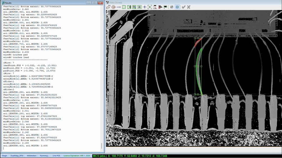
At the core of the measurement capability is Area Multi-Focus (AMF) 3D imaging. This technique performs a controlled Z-axis sweep, capturing images at discrete focal planes throughout the depth of the wire bond structure. Each image contributes in-focus information at a specific depth, and this data is combined to generate a dense 3D point cloud representing the full wire geometry.
Unlike extended depth-of-field techniques that collapse depth information into a single 2D image, AMF preserves true Z-height data. This enables direct, quantitative measurement of loop height, curvature, and spatial relationships between wires, bond pads, and leads, parameters that are difficult or impossible to assess reliably using 2D imaging alone.
Inspection routines are implemented in a flexible metrology software environment that supports scripting, custom logic, and advanced image processing. Capabilities include optimized edge detection for reflective features, histogram-based thresholding to isolate wires and bond pads, masking and blob analysis for continuity verification, and extraction of dimensional measurements for statistical process control and yield analysis. This flexibility allows routines to be tailored to specific wire bond designs, materials, and manufacturing requirements, supporting both development and high-volume production.
Performance Evaluation Through Measurement of Real-World Wire Bonds
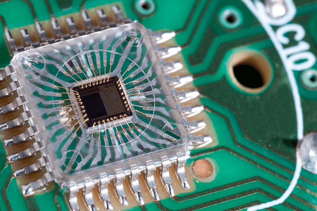
A test application was developed using a wire-bonded semiconductor device to evaluate system performance. Although the device was not representative of a product currently in production, its wire-bond structures closely resemble those found in a wide range of industrial applications.
The inspection routine evaluated wire continuity from pad to lead, bond placement accuracy on pads and leads, loop geometry and relative Z-height, detection of broken or missing connections, and wire-to-wire contact or overlap.
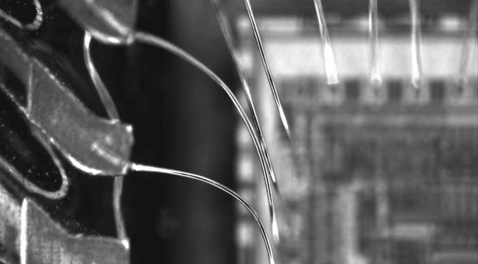
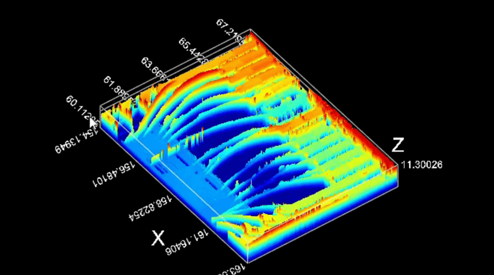
Using AMF imaging, the system generated three-dimensional grayscale representations of the wire bonds. Histogram-based feature detection established adaptive intensity thresholds, enabling reliable isolation of wire bond structures despite surface reflectivity variations. Blob detection routines then identified individual wires and verified continuity along their entire length.

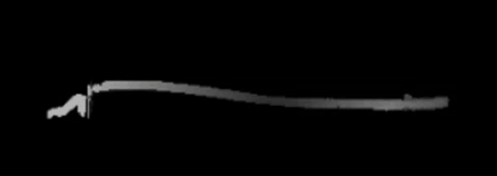
The resulting AMF point cloud enabled direct measurement of loop height and geometry. Because each wire segment was captured at its optimal focal plane, the system consistently resolved the apex of the wire loop, an area often poorly characterized by conventional inspection tools. Measurements were repeatable across multiple wires and insensitive to loop height variations.
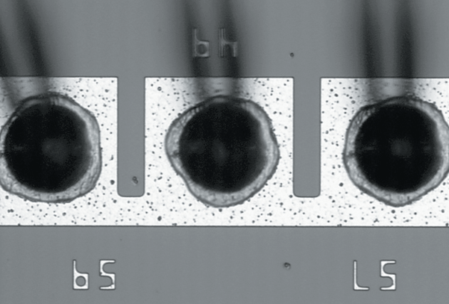
The routine also verified that each wire terminated within predefined pad and lead regions. Deviations from nominal placement were automatically flagged, enabling early detection of bonding process drift or equipment misalignment.
Measurement Accuracy, Traceability, and Transparency
Under standard optical configurations, the system reliably resolves features down to approximately one micron, meeting most wire-bond inspection requirements in high-volume production environments. Higher-magnification configurations support finer resolution for research, development, and failure analysis applications, with the expected tradeoff of reduced field of view and throughput.
All measurements are fully traceable through calibration to a certified line-scale bench referenced to national measurement standards. This traceability supports confidence in reported results and enables use in regulated industries such as automotive, aerospace, and other compliance-driven electronics markets.
As with all optical systems, features below the optical resolution limit cannot be measured reliably. Highly absorptive or extremely low-contrast surfaces may require specialized illumination or complementary inspection techniques. While the system delivers robust, non-destructive measurement at the micron scale, it is not intended to replace destructive analysis methods or electron microscopy for nanoscale defect characterization.
Beyond Traditional Automated Optical Inspection: True 3D Measurement
Compared with traditional automated optical inspection (AOI) systems, the optical metrology system evaluated provides true three-dimensional measurement of wire loops rather than inferred height. It also offers improved visibility of reflective wire surfaces, greater software flexibility to accommodate evolving designs, and quantitative measurement data suitable for process control and yield analysis.
Although 3D AMF inspections requires additional Z-axis scanning, and therefore exhibit lower throughput than simple 2D imaging, this tradeoff delivers substantially higher measurement fidelity and more reliable defect detection, particularly for complex loop geometries and subtle bonding anomalies.
From Inspection Data to Manufacturing Insight
Inspection results can be exported in standard data formats for seamless integration with external statistical process control (SPC) systems, yield analysis tools, and manufacturing execution systems (MES). The system’s open software architecture also enables straightforward integration with third-party platforms for trend analysis, process drift detection, and predictive process monitoring.
Custom operator interfaces can be developed to streamline shop-floor interaction by presenting clear defect indicators, pass/fail status, and summary statistics for production use. At the same time, full access to detailed metrology data is preserved, enabling deeper analysis by process and reliability engineers.
A Clearer VIEW of Critical Connections
Modern wire-bond inspection requires more than two-dimensional imaging and inferred measurements. True three-dimensional characterization is essential to accurately quantify loop geometry, bond placement, and electrical continuity — particularly for ultra-fine, highly-reflective wires.
Precision 3D AMF imaging, combined with flexible, software-driven measurement routines and advanced illumination, delivers quantitative, repeatable, and traceable results. Seamless integration with SPC, MES, and external analytics platforms further transforms inspection data into actionable manufacturing intelligence. These capabilities provide clear advantages for today’s IoT devices, power electronics, automotive electronics, and other high-reliability applications where yield, defect detection, and early process drift identification are critical.
As wire bonding remains central to demanding semiconductor applications, advanced optical metrology offers a scalable, future-ready inspection solution for both high-volume manufacturing and advanced engineering analysis.
To learn more about precision optical inspection solutions for wire-bond packaging, contact VIEW Micro Metrology or visit https://viewmm.com/en/.


