
By Lori Scott, Senior Director of Marketing, Intel Foundry
The Intel Foundry is redefining the scalability limits of artificial intelligence (AI) and high-performance computing (HPC). Intel Foundry engineers and collaborators highlighted breakthrough innovations — from Embedded Multi-die Interconnect Bridge-T (EMIB-T) enabling large multi-die systems without significantly increasing cost or manufacturing risk, to co-packaged optics (CPO) delivering dramatically higher bandwidth at reduced power in the near term, to future glass substrates that unlock larger form factors and improved stability.
Together, these technologies demonstrate Intel Foundry’s commitment to driving the next generation of packaging solutions to enable higher performance data center systems.
Advancing EMIB-T Scaling Capabilities
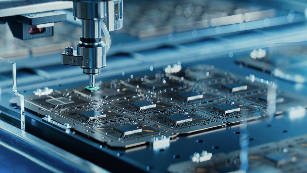
EMIB-T advanced packaging technology enables ultra large, high-performance chiplet systems that scale beyond silicon reticle limits and traditional packaging constraints. EMIB-T leverages embedded silicon bridges for high-density lateral 2.5D interconnect, combined with through-silicon via (TSV)-enabled vertical scaling to enhance power delivery. This approach allows Intel Foundry to construct package-scale systems that function as a single large device while being composed of many optimized chiplets. These advances help customers increase package sizes and support high bandwidth logic-to-high bandwidth memory (HBM) interconnects for demanding AI and HPC applications.
We share a wide range of EMIB-T advanced packaging capabilities that allow customers to scale performance without increasing cost, risk, or power disproportionately.
Scaling EMIB-T advanced packaging technology to meet HPC and AI demand: Intel Foundry engineers demonstrated how to scale the first layer interconnect (FLI) bump pitch down to 25 µm, increase package form factor sizes up to 120 x 120 mm, and integrate more than 9x reticles of compute and memory Si content on a single package. With co-optimized signal and power integrity delivering over 12 Gb/s for HBM4e and 64 Gb/s Universal Chiplet Interconnect Express (UCIe) interface performance, EMIB-T enables customers to disaggregate large AI systems into optimized chiplets while achieving near-monolithic performance for accelerators, servers, and HPC platforms.
Other EMIB-T research by Intel Foundry and collaborators included:
- Collaboration with Siliconware Precision Industries: 3D integration of SRAM chiplet in fan-out embedded bridge
- Enabling over 12 Gb/s HBM4e with EMIB-T
- Package architectures for hyper large form-factors for AI and HPC
- Challenges and solutions for package-level ultra-large die complexes
Co-Packaged Optics for Improved Bandwidth
CPO addresses several fundamental system-level problems that arise when data center bandwidth scales faster than electrical interconnect technology can support. By moving optical‑to‑electrical signal conversion directly to the package, CPO enables higher bandwidth, lower power, and more scalable systems.
High-performance detachable edge optical connector: Intel Foundry engineers are developing CPO technologies that can effectively convert these signals with pluggable solutions. Our edge-coupled optical interface uses glass fan-out couplers and expanded-beam edge connectors to deliver low-loss, highly reliable, and detachable optical interfaces that are compatible with high volume manufacturing. Suitable for wafer level and package level assembly, this architecture will potentially enable energy efficient, high bandwidth AI scale-up networks in compact, serviceable systems.

V-groove based edge coupling glass coupler interface: Our engineers have found a new, more robust way to connect optical fibers to photonic chips inside a CPO package. Traditionally, CPO edge coupling connects fibers directly to silicon photonic chips using fiber array units (FAUs) inserted into V-grooves etched into silicon, which is a difficult and fragile process. Intel Foundry replaces the fiber-only approach with a rigid optical glass coupler that attaches to the V-grooves in photonic integrated circuits (PICs). This method could simplify manufacturing for CPO by improving bandwidth and energy efficiency while reducing latency.
Other CPO research from Intel Foundry included:
- Die-to-die attach with low thermal input thermo-compression bonding
Next-Gen Glass Substrates for Larger Package Sizes
Traditional organic core substrates are reaching their limit for scaling. As packages integrate more chiplets and compute demands rise, significant improvements are required in signaling speed, power delivery, design rules, and substrate stability. Intel Foundry’s research and development on glass core substrates focuses on removing this base material as a scaling bottleneck. Glass enables higher performance heterogeneous integration, better power delivery and stability, and low warpage for large AI and HPC packages. As a foundational technology for next-gen advanced packaging, the future developments on glass substrates provide electrical and optical integration on one platform.
Glass core substrate advanced packaging for AI and HPC: Intel Foundry’s research on glass substrates with advanced through-glass vias (TGVs) is another step into the future of this technology. Similar to through-silicon vias used in silicon interposers and 3D stacking, TGVs serve a similar vertical connect purpose in glass substrates. Intel Foundry can precisely and repeatably create many types of vias in glass — from low taper TGVs to mixed TGV sizes to cavities for embedding devices — enabling flexible package designs. Engineers showed that fully copper-filled TGVs can survive very harsh thermal cycling without failure, demonstrating long-term reliability. While organic substrates warp and shift during processing, glass stays flat and stable, allowing extremely precise alignment between layers. This directly supports continued scaling for multi-chiplet systems.
To learn more about Intel Foundry’s advanced packaging solutions, visit intel.com/foundry or reach out to us at foundry.contact@intel.com.


