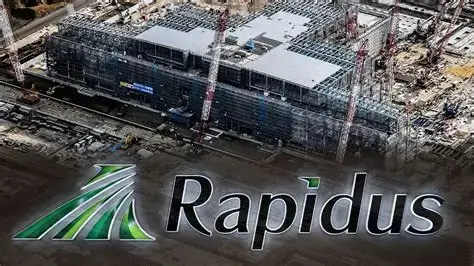
AI is transforming the next-generation advanced foundry for 2nm chips, thus reshaping the semiconductor industry, writes Rozalia Beica.
The semiconductor industry is entering a historic inflection point, one driven by unprecedented demand, geopolitical shifts and the rise of AI. As nations re-evaluate their technology strategies and companies strive to localise advanced manufacturing, the traditional foundry model is being pushed to its limits.
AI sits at the centre of this transformation. Its rapid adoption across datacentres, edge systems, autonomous platforms and industrial automation has unleashed explosive demand for high-performance, energy-efficient chips. Gartner forecasts nearly 30% annual growth in AI semiconductor revenue, while McKinsey predicts the need for three to nine new advanced-node fabs just to meet global demand.
This convergence of escalating costs, supply chain reconfiguration and technology acceleration has created a ‘perfect storm’ and a unique opportunity to redefine semiconductor innovation.
When scale slows speed
For decades advanced semiconductor manufacturing has been concentrated among a few dominant players. While this brought efficiency and scale, it has also constrained agility. Traditional fabs, optimised for predictable, high-volume output, struggle to support the rapid experimentation required for AI, HPC and emerging chiplet architectures.
The resulting innovation gap is not just technological; it is structural. The industry needs a new model of manufacturing, one that is intelligent, adaptive and inherently collaborative.
A smarter, faster paradigm
The concept of the AI Foundry embodies this shift. It is a manufacturing ecosystem that continuously learns, senses and adapts, embedding intelligence from design through fabrication and packaging. By integrating AI into materials, processes and equipment control, such a foundry can:
- Predict performance and yield deviations
- Optimise equipment behaviour dynamically
- Shorten development and qualification cycles
- Enable rapid design–manufacturing co-optimisation.
Rapidus has built its mission around this philosophy. Focused on 2nm and next- generation packaging technologies, the company is designing a sensor-rich, data-driven environment under its Innovative Integrated Manufacturing framework. Through global collaboration with governments, academia, suppliers and design partners, Rapidus is building a platform that accelerates innovation from early design concepts to system integration.
Speed as the new strategic advantage
In the AI era the most precious resource is time. Companies that can iterate fastest will lead. Where traditional fabs may take up to a year to qualify a design, Rapidus is developing an ecosystem that dramatically shortens these cycles. AI-enabled co-optimisation, real-time process feedback and fully integrated wafer-to-package operations eliminate silos and accelerate productisation.
This approach empowers innovators, startups, research groups and companies building novel architectures, to move from concept to manufacturable product far faster than legacy infrastructures allow.
New levels of system performance
As Moore’s Law slows, advanced packaging has become the new frontier of semiconductor differentiation. The ability to integrate heterogeneous components — logic, memory, RF, photonics — within a single package enables architectures optimised for power, latency and functionality. Rapidus positions packaging as a core pillar, not an afterthought. By co-locating 2nm fabrication with advanced 3D integration and chiplet assembly the company delivers a seamless path from wafer to complete system. For AI and HPC workloads that demand ultra-dense interconnects, superior thermal performance and efficient power delivery, this integrated approach is essential.

Innovation through collaboration
Rising costs and technical complexity have increasingly excluded smaller players from accessing advanced manufacturing. Combining startup agility with national mandate and global partnerships, Rapidus is creating an open, flexible environment where new ideas can be tested and scaled.
Through deep collaboration with equipment vendors, materials suppliers, design houses and research institutions across Asia, Europe and the US, Rapidus acts as a global enabler, strengthening innovation pathways and supply chain resilience.
Sustainability by design
As demand for advanced chips grows, so does the industry’s environmental footprint. Rapidus is addressing this challenge early, embedding sustainability into both process design and facility operations. Its strategy includes:
- Integration of renewable energy
- Process and equipment optimisation for energy efficiency
- Water and material usage reduction
- Low-power device architectures at the 2nm node
- Exploration of large-panel manufacturing to improve resource efficiency.
At Rapidus, sustainability is not a constraint, it is a foundation for long-term competitiveness.
Redefining the foundry
Semiconductors have become the invisible infrastructure that powers modern economies. But the next era will not be defined solely by transistor scaling; it will be defined by how intelligently and collaboratively we design and manufacture them. Rapidus represents a new foundry archetype, one that fuses national vision, global collaboration, advanced technology and startup agility. It is building not only fabs, but an entirely new model of manufacturing in which speed, intelligence and sustainability converge.
By closing the innovation gap, Rapidus aims to create a more diverse, dynamic, and resilient semiconductor ecosystem, one capable of keeping pace with the intelligence it helps create.
By Rozalia Bieca, Rapidus CTO of Packaging Technologies
Full Blog from: Electronics Weekly, Accelerating 2nm & advanced packaging through global collaboration | Electronics Weekly