This year’s annual International Microelectronics Assembly and Packaging Society (IMAPS) Device Packaging Conference (DPC) in Arizona was bursting with excitement and acted as a platform for the industry’s brightest engineers, researchers, suppliers, and students from across the microelectronics packaging ecosystem to come together to share innovations shaping next-generation computing systems.
With record attendance again this year, surpassing 1,080 participants, the conference served as a major gathering point for the advanced semiconductor packaging community and a platform for technical exchange across the industry.

This year holds additional significance as it marks the first event following IMAPS’s acquisition of 3D InCites content platforms and expanding the Society’s role as a central hub for knowledge sharing within the advanced packaging ecosystem. I am honored to write this first conference coverage to help open this new chapter of IMAPS’s digital platform.
This experience provided a unique vantage point to observe how ideas move throughout this ecosystem–reinforcing the central theme of the conference: innovation in advanced packaging is fueled as much by collaboration and the exchange of expertise as it is by technological advancement and IMAPS is the place to find both.
AI Infrastructure Growth – Bubble or Structural Shift?
At a conference full of engineers, the numbers naturally take center stage, and this year’s figures were both astounding and revealing of the market trends shaping the industry. Let’s explore a brief rundown.
Preet Virk is the SVP & General Manager, Photonic Fabric BU, Marvell, as part of the Global Business Council’s Plenary Session, explored how data center Capital Expenditure (CAPEX) spending is up nearly $400 billion over 2023. Tech giants, like Marvell, are spending an unprecedented amount of money to build, expand, and equip data centers for AI infrastructure.
Is this another telecom bubble? Virk addressing this explained, “the difference is today’s CAPEX is being funded by free cash flow–these investments are being made with organic revenue, and they’re already paying off. Because of that, this cycle is likely to continue for a very long time.” AI is more than ever booming, relevant, and far from its end.
The demand for AI is driving such expenditure, with ChatGPT alone receiving roughly 700 million users by the end of 2025, 4x that of the previous year. Likewise, “over 92% of Fortune 500 companies used AI technology by the end of the same year,” said DPC keynote speaker Thorsten Meyer of Infineon. The demand is clearly widespread and rapidly expanding, with outstanding adoption rates higher than nearly any technology or service in history.
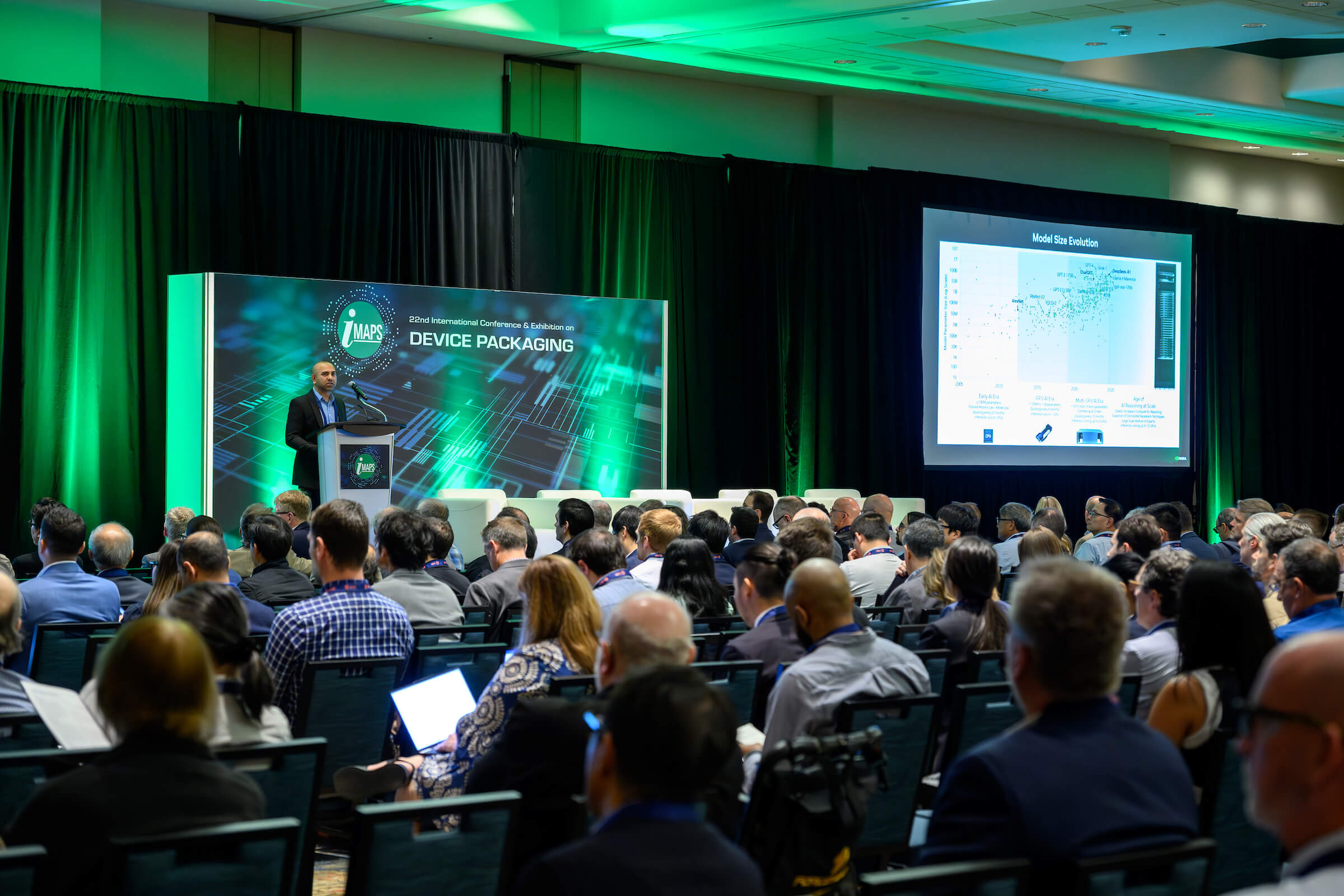
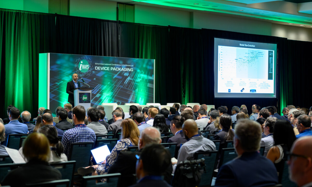
These booming adoption rates provide a strong incentive for companies to sustain this growth, investing extraordinary sums in AI infrastructure. DPC keynote speaker, Sandeep Razdan from NVIDIA, noted that in a data center, each GPU has an estimated Total Cost of Ownership (TCO) of $2.50 per hour for the data center operator. At hyperscale this becomes significant, amounting to roughly $1.125 million per hour for a facility to run.
At this scale, cost is no longer just a function of compute, but of power, efficiency, and system design. This places increased pressure on the industry to reduce energy consumption and improve performance. As a result, advanced packaging and system-level innovations are becoming critical levers for managing cost and scalability in infrastructure.
That scale of investment illustrates why many experts describe the current AI surge as an “infrastructure-first” shift, where companies are prioritizing investments in data centers, specialized chips, and power systems before expanding consumer-facing applications.
So, is this “bubble” at risk of bursting? Unlike past technological cycles, today’s investments are supported by strong organic revenue and are being directed toward foundational infrastructure: data centers, power systems, and advanced chips.
At the same time, user adoption continues to grow, with many consumers and enterprises willing to integrate AI into their daily workflow and take on subscription models. As semiconductors and AI increasingly serve as a production layer for the global economy and core in future technologies, concerns about an imminent “bubble” appear less pressing.
Scaling AI – From Scale-Out to Scale-Up
The primary constraint on continued AI expansion is the ability to build and power the infrastructure required to run it. The latest development is AI-era scaling: as model complexity grows roughly 10x in parameters annually, data center architectures are shifting from traditional scale-out designs toward scale-up systems.
Brandon Hoff, leader of the International Data Corporation’s (IDC) datacenter research Enabling Technologies Team during the Global Business Council’s Plenary Sessions, explained how modern AI workloads are being trained on clusters containing tens of thousands of accelerators, with some deployments approaching 100,000 GPUs operating within a single training environment.
At this scale, the traditional scale-out–adding more servers–architectural approach is no longer sufficient. Now, there is a shift towards scale-up–adding more GPU/memory to a single node–that places greater emphasis on innovations in advanced packaging, interconnect technology, and system integration. What once existed across the entire circuit board is moving evermore into the package itself.
Power and Efficiency as a Remaining Constraint
The compute used to train large AI models has doubled approximately every 3.4 months. This rapid growth far exceeds the pace of hardware improvement predicted by Moore’s Law, which historically estimated a doubling of transistor density every two years. In response, the industry is forced to focus not only on the scaling compute, but on managing the immense power demands that accompany it.
The numbers illustrate the challenge clearly: a single ChatGPT query is estimated to require roughly ten times the energy of a Google search, while training large AI models can consume energy equivalent to the output of approximately 25 wind turbines. Likewise, 330 million metric tons of CO2 were emitted by data centers in 2020, nearly 3x that of Finland in the same year. Keep in mind, this was prior to the major inflection in AI usage beginning 2022.

There is clearly no AI without a massive toll on the power grid. And “increasing energy efficiency, especially via thermal efficiency, is one important lever to reduce consumption of AI data centers,” Thorsten Meyer of Infineon explained.
One emerging approach discussed during the conference was the advancement of co-packaged optics, a technology designed to significantly reduce the power consumed by data movement in large AI and machine learning clusters.
During his discussion, Sandeep Razdan of NVIDIA explained how integrating optical interconnects directly with compute packages can improve both energy efficiency and bandwidth within large-scale systems. While many in the room initially viewed the technology as an advancement still years away, attendees were surprised to hear that NVIDIA has already begun implementing these concepts to address the growing power and bandwidth demands of next-generation AI infrastructure.
In conclusion, the future system design of scale-up architecture will be defined by how efficiently computing power can be delivered, cooled, and managed.
Community Knowledge and Exchange
Moving away from the numbers, DPC classically brought about the picture of community that the assembly and packaging ecosystem never fails to express. Knowledge exchange is at the forefront of tackling these problems, and the semiconductor community stays open and committed to collaboration.
The technical sessions brought about the industry’s brightest, sharing topics from advanced packaging structures, glass core substrates, small body fanout packaging, interconnect methods, and much more. These technical sessions highlight a fascinating depth of knowledge where students, researchers, and industry professionals alike share their passion through 30-minute deep-dives into the most cutting-edge technology the world can offer.
Each company and individual attendee have a unique piece of the pie, and I came to realize that each advancement needed another to progress the industry. ASE’s Wiwy Wudjud defined the collaborative spirit well when talking about reliability testing for wafers. She explained that these advancements are made “to improve the entirety of the semiconductor ecosystem”. Comments such as this reflect the community-oriented nature of IMAPS events, along with the fact that advancement happens uniquely as a “whole” in this industry.
Informal conversations throughout the week reinforced this cooperative nature. While walking through the exhibit hall–featuring 88 companies–I had the opportunity to speak with representatives from a wide range of organizations, including teams from Amkor Technology to Deca. Curious to learn more about their technologies and software platforms, I found that many were eager to share additional insights and expand on the technical sessions they had presented earlier at the conference.
Conversations with the team from Amkor highlighted the company’s continued U.S. expansion, including its planned advanced packaging facility in Peoria, Arizona—roughly $2 billion investment expected to span more than 100 acres, very near to where DPC takes place.
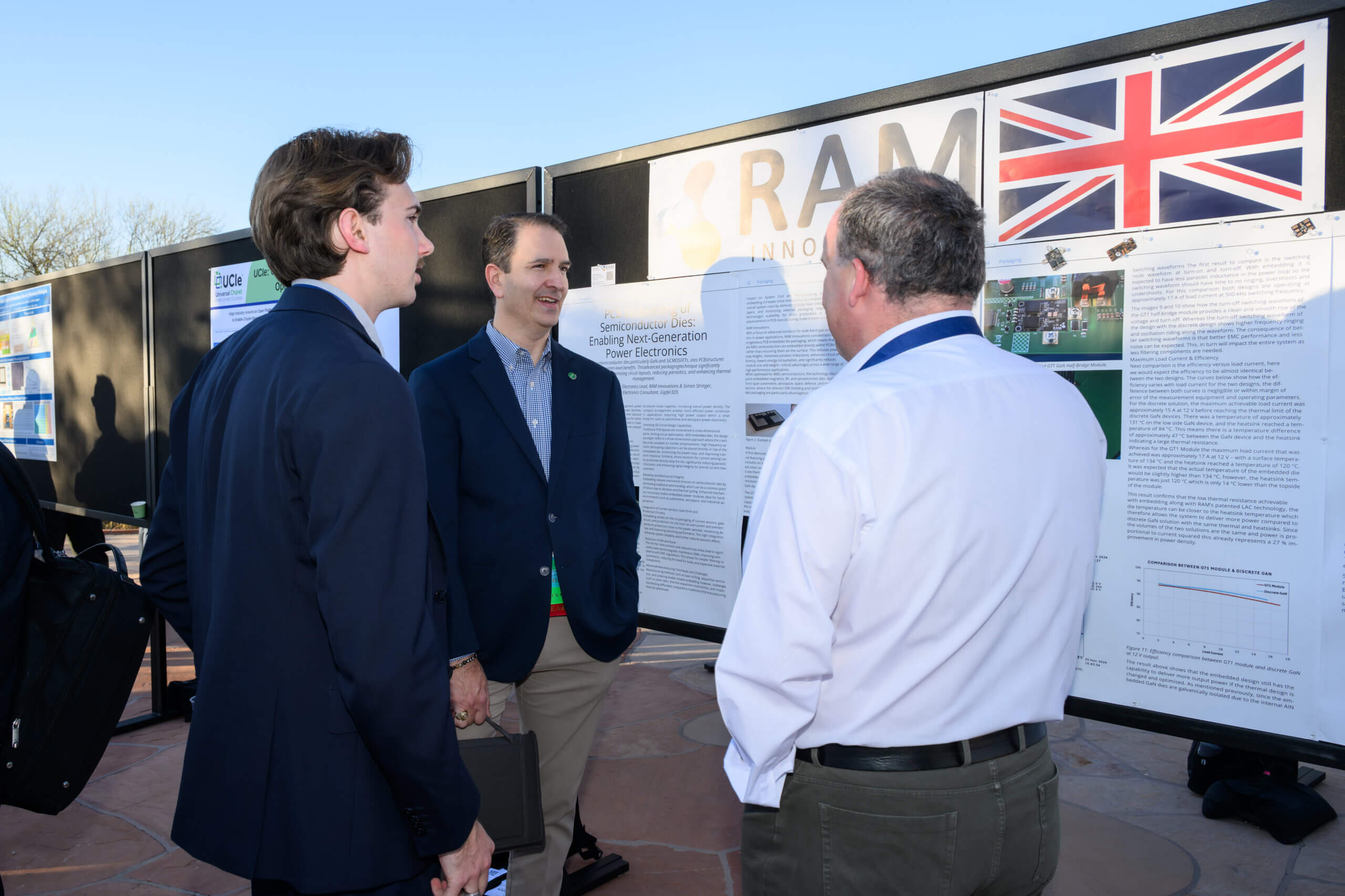
The poster sessions went one step further to illustrate knowledge transfer across generations of engineers. Students from various universities, such as ASU, were able to share their research with companies to present potential breakthroughs and recent discoveries.
One moment stood out when an industry professional listened intently to a student’s poster presentation and offered thoughtful suggestions on how the research could be refined to improve heat dissipation results. It was a small but powerful reminder of how guidance and support flow naturally within this industry.
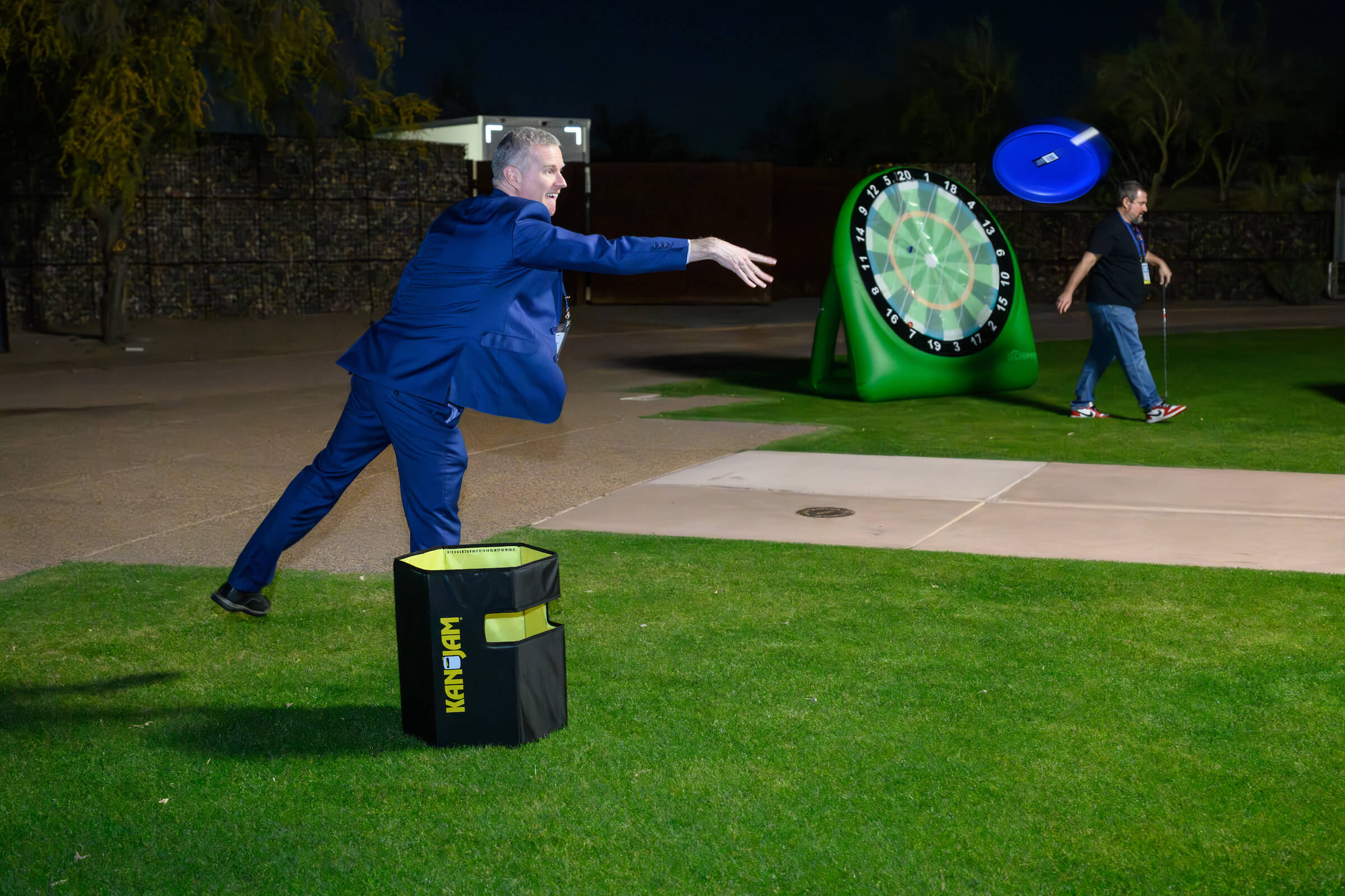
Besides serving as a platform for knowledge transfer, IMAPS conferences are also known for fostering a strong sense of community. I had the opportunity to get out of the conference rooms and outside to participate in the Backyard Olympics, where attendees gathered for friendly competition while raising money to support the IMAPS Microelectronics Foundation. Proceeds from this fundraiser went directly to its new 3D InCites Scholarship supporting women in STEM. There was fierce competition and the opportunity to network, collaborate, and enjoy the time in Phoenix during the conference.
Conversations with peers during the activities and Welcome Reception from organizations such as IBM, ASE, Deca, Amkor, Cadence, ACM Research, and IMAPS expressed the continued receptivity and collegial spirit that these conferences foster.
With the integration of 3D InCites into the IMAPS ecosystem, that same community-driven exchange of ideas now has an opportunity to extend beyond the conference halls, made digital year-round. IMAPS provides an environment where both professional relationships and technical insights can grow, and I am already looking forward to the next conference and reconnecting with the many colleagues and friends made throughout the DPC.
About the Author: Camden McCrea has been a writer with 3D InCites for the past two years, covering the microelectronics assembly and advanced packaging ecosystem and traveling internationally to engage with industry leaders and emerging research across the global semiconductor industry.