

For decades, Moore’s Law has been a way to measure performance gains in the semiconductor industry, but the ability to double the density of transistors on a chip every two years is becoming increasingly challenging. With scaling reaching its limit, manufacturers are looking to advanced packaging innovations to extend the performance gains that the industry, and the world at large, have grown to depend on. Cu-to-Cu hybrid bonding is one way the industry is looking to extend ever-increasing I/O density and faster connections, all while using less energy.
Primarily used in CMOS image sensor (CIS) devices today, hybrid bonding is poised to be the successor to microbumps in devices requiring high-bandwidth data transfer, particularly those designed for artificial intelligence (AI), high-performance computing (HPC) and graphics processor units (GPUs). However, microbumps are increasingly problematic at pitches under 10µm. A very small non-uniformity in the plated microbump height or variation in the solder reflow process may be negligible when the bump structures are large, but with fine-pitch microbumps, these small variations can lead to bad joint formation and affect the electrical yield. The end result: defective dice and packages.
Another challenge for scaling microbumps is that at such fine pitches, the solder of the bump may bridge, causing shorts. In addition, controlling the plating uniformity of these small structures is challenging, while the ability to find new, more suitable underfill materials to fill the shrinking space between the microbumps is also required.
The direct, fine-pitch Cu-to-Cu interconnects enabled by hybrid bonding will allow for 1,000 times the number of connections as microbumps. But as with all innovations, hybrid bonding poses challenges even as it enables higher-performance AI, HPC, GPU, and image sensors. Surface cleanliness, for one, is paramount.
A less-than-1µm particle on the bonding surface of an interconnect with a pitch that is less than 10µm will likely create a void in the bonded structure and impact the yield of the final device. However, on an interconnect of greater size and pitch, a 1µm particle would have a negligible impact on the process yield. For these reasons, advanced packaging facilities must use clean room standards approaching the front-end fab level, along with inspection tools to discover sub-micron particles and defects.
Other areas of concern include the warpage of the thinned wafer, alignment errors of the bonding surfaces, precise control of Cu pad height, and the generation of the divot-like gap that is filled by the bonding of the two Cu pads through thermal expansion. As such, high-performance metrology tools must be used as well.
In this article, we will discuss the trends leading to hybrid bonding, the challenges facing hybrid bonding, and the tools that provide the best solutions.
Why Hybrid Bonding?
The reasons for the transition to hybrid bonding, as opposed to microbumps, are fairly straightforward. 3D memory stacks and heterogeneous integration — two players in the More than Moore era — require extremely high-interconnect density. This is a need for which hybrid bonding can deliver. Compared to micro-bumping, which itself supports a high-density interconnect scheme, hybrid bonding delivers smaller dimension I/O terminals and reduced pitch interconnects. The standoff distance between each die is dependent on the height of the microbump, but this distance is nearly zero with hybrid bonding. As a result, hybrid bonding interconnect schemes can reduce the overall package thickness considerably, perhaps even as high as hundreds of microns in multi-die stack packages.
There are currently three approaches to hybrid bonding: wafer-to-wafer (W2W), one-by-one die-to-wafer (D2W), and collective D2W. With W2W bonding, two wafers are directly bonded to each other. This is a common method for backside illumination technology (BSI) architectures for CIS. With one-by-one D2W bonding, the die transfer uses a flip-chip bonder from a carrier to a destination wafer. With collective D2W, the dice are attached to a carrier wafer leading to the W2W bonding of reconstructed and destination wafers.
Today, hybrid bonding has been proven to be feasible in the high-volume manufacturing of 3D NAND stacks and 3D systems on a chip (SoC). Research and development are ongoing regarding the application of hybrid bonding in high-bandwidth memory (HBM), as well as other 3D integration applications when microbump pitch is less than 10µm.
The Hybrid Bonding Market
From 2021 to 2027, the high-end packaging market is expected to grow by a CAGR of 22% based on the production wafer volume forecast from the Yole Group. These high-end applications include 3D NAND, 3D SoC, HBM, and 3DS, Si interposer/bridge integration, and ultra-high-density fan-out packages.
The adoption of hybrid bonding is at various phases for these high-end applications. Currently, 3D memory stacks are a volume driver for hybrid bonding and should remain that way, while 3D NAND is initially being adopted, a move that should be followed by HBM. In addition, the initial 3D SoC products that will use is unclear. We expect to see the rollout of more devices utilizing hybrid bonding in the next two to three years.
Challenges and the Process Control Needs
Although the performance-gain promises of hybrid bonding are all but certain to lead to the increased use of the bonding technique in the market, especially in high-performance computing, data center networking l and autonomous vehicles, the challenges posed by this emerging technology are significant to both assembly and testing. Overlay errors and yield-killing void defects are heightened problems, while electromigration, delamination, and copper diffusion greatly impact reliability.
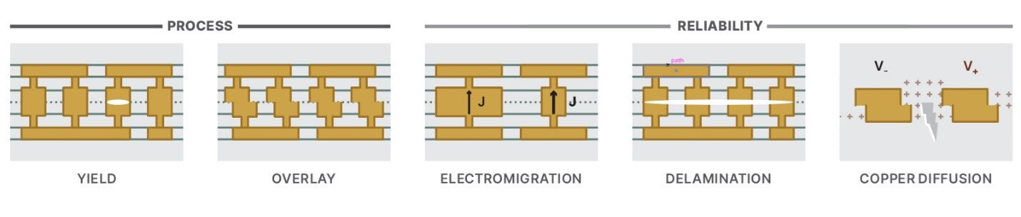
Not surprisingly, one of the more significant challenges at the pre-bonding step of hybrid bonding involves the interconnection of the two Cu pads that are to be joined. For the process to work and for the two pads to be successfully bonded, chemical mechanical planarization (CMP) must be used to ensure that the Cu pads have a suitably small surface recess into the oxide. This allows the two Cu pads to expand and touch, and eventually bond through the annealing process, while not unzipping the previously formed dielectric-dielectric bond around the Cu pads.
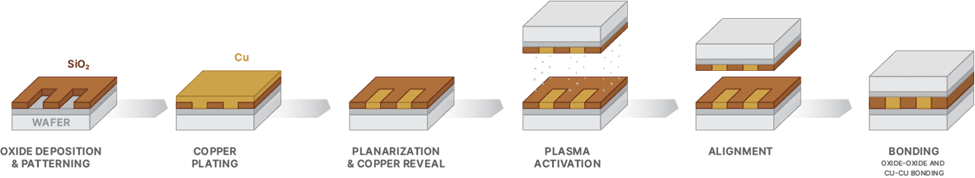

With all of this in mind, establishing and maintaining tightly controlled electroplating and CMP processes is necessary. Without such stringent controls, the bonding will not succeed and HVM will not be feasible. To accomplish this, high-precision, high-throughput metrology measurement, and control techniques are required to monitor the dielectric film and Cu thickness, as well as surface topography.
Particle control is a mandatory yet difficult part of the hybrid bonding process because so many back-end processes are prone to generating debris. These back-end processes include wafer grinding, wafer-edge trimming, wafer sawing, and taping/de-taping. While traditional back-end inspection requires defect sensitivity greater than 5µm, hybrid bonding requires a surface defect detection that is significantly less. Tools designed to meet the standards of hybrid bonding defect detection must have greater resolution and speed to detect these nanoscopic defects. Once the two Cu pads are bonded, failing to identify the critical size particles significantly increases the probability of creating voids 10 times or larger than the initial sub-micron particle.
During the hybrid bonding process, several key process steps bring different challenges and obstacles. In addition to the problem with particles and surface topography after CMP, other challenges include die cracks and wafer warpage. The post-CMP total thickness variation of the dielectric film across the wafer can also affect the bonding process. As a result, back-end fabs will need metrology tools for film thickness measurement, in addition to high-throughput inspection tools for die-level crack/particle detection.
Lastly, in the post-bonding stage, both inspection and metrology tools continue to play a crucial role in process control. These tools will need to measure bond line thickness and pad alignment and be able to identify voids. A high-speed infrared inspection system will be useful in identifying voids and other defects, but there are limitations when applied to identifying voids under metal.
Only known good die will be subject to hybrid bonding, and in the case of multi-die stacked 3D packages, such as HBM, this process must be repeated multiple times. Given the complexity and stringent requirements, tight process control is critical along each step of the stacking process. Analytics software capable of tracing the genealogy of each die and each process step can bring invaluable information for yield enhancement.
Conclusion
The use of Cu-to-Cu hybrid bonding is moving beyond CIS devices as it is adopted for 3D NAND and 3D SoC. Even more applications are on the horizon. But this potential building block of the More than Moore era has significant challenges. For hybrid bonding to be successfully implemented, a wide range of tools is needed. Metrology tools can be used to measure pre- and post-CMP dielectric, Cu film thickness, and topography, as well as identify metal film stack voids. Inspection tools can be used to detect particles, cracks, and voids, whereas tools with infrared capabilities may have an advantage. Inspection tools can also be used to measure residual Si thickness and inspect the backside after thinning. Last but not least, analytics software can also be employed to enable chiplet and process traceability.
With these solutions and processes in place, hybrid bonding should see further and, possibly, rapid implementation, bringing with it performance gains to servers and networking switches, AI/ML and AR/VR, and autonomous vehicles.
Editor’s Note: This article first appeared in The 2023 3D InCites Yearbook. Read the issue here. For more on Hybrid Bonding, check out our coverage from ECTC 2023, and listen to this recent podcast episode featuring Monita Pau.
;

