
With over 350 papers in 36 oral sessions and 5 interactive presentations, there was no shortage of content to absorb at the 2023 Electronics Components Technology Conference (ECTC 2023), which took place May 31-June 2 in Orlando, FL. The keynote and panel sessions discussed technical topics including quantum computing, chip-to-wafer hybrid bonding, advanced packaging for harsh environments, high-density substrates, mm-wave phased-array packaging, and photonics.
In addition to purely technical topics, we were updated on the CHIPS for America Act, and how to diversify our technical workforce. Running in parallel to technical sessions on Tuesday was a full-day Heterogeneous Integration Roadmap Workshop. With so much opportunity to learn, it’s no wonder this year’s conference had near-record attendance, with 1616 registrants. (The highest in-person attendance was 1,738 in 2018 San Diego).
Although I spent most of my time podcasting, I did manage to attend the keynote talk and some of the panels that addressed key areas of interest. But before I recap some key takeaways, I want to talk about the changes at ECTC that made this year’s event the best I’ve ever attended.
New Venue, New Format
If you remember the last time ECTC took place in Orlando Florida (2017 – BEFORE COVID), you may recall my less-than-pleasant experience at the Swan and Dolphin. If not check it out here – the first paragraph tells the story. In my opinion, one of the only good things about COVID is that we got to skip Orlando altogether in 2020. So you can imagine my delight when the ECTC executive committee decided not to renew its contract with the Swan and Dolphin. Instead, they upped their game and landed on the JW Marriott Grand Lakes Resort as the site to host three of the next nine ECTCs.

My room was spacious, airy, and clean. The bed was comfy. I didn’t have to walk miles to get to the conference center. The food was good. And on Friday, I played hooky to enjoy the Lazy River and waterslide for half the day; what a great way to wind down from a non-stop week. The committee gets high marks for this choice. I’m sure they won’t have a problem coaxing this year’s attendees to return three years hence.
The new venue for 2023 wasn’t the only logistical change. ECTC’s practice is to lock into a nine-year plan, rotating between three locations. For the other two, they signed a contract with Gaylord Hotels in Denver (2024) and Dallas (2025). I’m told we’re going to love them.
Under the leadership of Ibrahim Guven, this year’s general chair, and Florian Herrault, the program chair, the committee also made some great decisions that improved the format. For the first time, instead of having the keynote speaker present during lunch on Wednesday, they opted to kick off the day with a keynote session. The result? A packed audience who actually listened to the keynote speaker. It’s hard to compete with 1500 noisy diners who are focused on the networking opportunity. It’s too bad that other speakers and award presentations were drowned out by attendee chatter. Maybe something else to consider moving next year? Just a thought.
The other brilliant decision was to move the evening plenary sessions (all but one) to Tuesday – in parallel with the HIR Workshop and Professional Development Courses. Because really, after a full day of conference followed by a reception, who wants to go back into a 7:15-9:30 session? I recall these being lightly attended by only die-hard attendees. Again – a round of applause for the executive committee. Change can be good!
Quantum Computing Needs Heterogeneous Integration
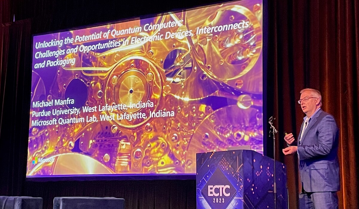
This year’s keynote speaker, Michael J. Manfra, delivered a talk entitled, Unlocking the Potential of Quantum Computers: Challenges and Opportunities in Electronic Devices, Interconnects, and Packaging. His official title is as long as my arm:
- Bill and Dee O’Brien Distinguished Professor of Physics and Astronomy
- Professor of Electrical and Computer Engineering
- Professor of Materials Engineering
- Scientific Director, Microsoft Quantum Lab West Lafayette
When it comes to talking or writing about quantum computing, I am way out of my league. It was somewhat comforting to know that most of the audience, save the physics experts, were in the same boat. Understanding this, Manfra tried to keep it at a high level. Here’s what I understood.
Why do we need quantum computing?
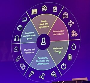
While it seems like it’s a niche technology, Manfra explained that quantum computing has real-world implications for accelerating scientific discovery. For example, 96% of all manufactured goods rely on chemicals and material science. From that perspective, quantum computing has the potential to touch every industrial sector, impacting 100% of humanity (Figure 1).
“For challenges that depend on computing power, it can address a subset of issues,” he explained. “It is excellent for small data problems with super polynomial speed up.”
Translation: Quantum computing addresses data problems that classical hardware cannot address. Qubits – not transistors- process information. Qubits are the analog state of the transistor and are more sensitive than classical analog. Practical problems require millions of qubits to complete long calculations. Therefore, we need millions of qubits to make a real-world impact.
Challenges and opportunities
Here’s the catch — quantum computers operate at extremely cold temperatures – in the 4 Kelvin range. Making qubits scalable and being able to control them at room temperature requires significant advancements in low-temperature electronics, packaging, and interconnection schemes.
Manfra described three types of qubit architectures: Silicon spin qubits, topological qubits, and transmon/photonic qubits. The key takeaway for this audience was that heterogeneous integration schemes, such as multichip modules (MCMs) and system-in-package (SiP), hit the sweet spot for topological qubits.
Some of the big challenges this community needs to address to bring quantum computing out of the lab and into manufacturing are power and thermal management solutions, as well as materials that can make qubits operate at a higher temperature.
From the perspective of the advanced packaging community, I expect the trillion-dollar question to be: Will there ever be volumes of quantum devices needed to make it a profitable investment for the packaging community? Also, another thought that occurred to me as I write this – will quantum computing negate Moore’s Law, as it doesn’t use classical transistor technology?
I had the opportunity to interview Manfra for our ECTC podcast episode (See below). He gets into a much deeper explanation than I do here.
The Password is Hybrid Bonding
For the second year running, hybrid bonding was the darling of the technical sessions. The joke going around the conference was that if hybrid bonding was in the title, the paper was accepted. That’s no surprise to us at 3D InCites. We’ve been talking about hybrid bonding for years and know what a game-changer it is for the microelectronics industry.
![[err-ad-fallback-title]](http://www.3dincites.com/wp-content/plugins/a3-lazy-load/assets/images/lazy_placeholder.gif)
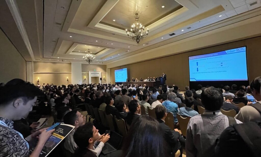
I attended the session, Copper Hybrid Bonding Interconnections for Chip to Wafer Applications. Moderated by Jan Vardaman, the line-up of speakers included Eric Beyne, imec; Xavier Brun, intel; Abhijeet Chakraborty, Synopsys; Raja Swaminathan, AMD; Thomas Uhrmann, EV Group; Chris Scanlan, Besi; and Andrzej J. Stojwas, PDF Solutions.
Beyne kicked it off with a discussion comparing wafer-to-wafer (W2W), die-to-wafer (D2W), and die-to-die (D2D) schemes. He noted that hybrid bonding is needed for high-density interconnects. While D2W is in production, Beyne noted that it could be 5-10 years before we reach wide adoption.
Swaminathan explained that hybrid bonding offers 3X the energy efficiency and 15X interconnect density over other advanced interconnect approaches and enables the future of scaling through chiplets, which is why AMD has leveraged it in its Ryzen 3D product family. Figure 2 shows AMD’s Instinct™ MI300 the world’s first data center integrated CPU+ GPU enabled by 3D advanced chiplet packaging – presumable thanks to hybrid bonding.
Providing the perspective of the design community, Chakraborty said that the future of 3D stacking and hybrid bonding will depend on through-silicon-via (TSV) pitch and hybrid bonding integration schemes. Multi-scale design process optimization is needed to manage warpage and interconnect reliability. Bottom line – next-generation 3D architectures need next-generation EDA tools.
Brun introduced a new phrase to our ever-growing lexicon — quasi-monolithic chips. These are heterogeneously integrated chip stacks using hybrid bonding. If we want to leverage hybrid bonding for external IP/die integration, he said we’ll need standardization of the bond interface. We also need system technology co-optimization (STCO).
Brun also highlighted remaining challenges that must be solved before we see wide adoption of C2W hybrid bonding. These include the cost challenge; yield challenges such as alignment accuracy, warpage, and coplanarity; and test challenges. He said we need a new test strategy for fine-pitch, multiple devices. Manufacturing challenges include a need for inline metrology, artificial intelligence/machine learning (AI/ML) training integration, and high-speed localized non-destructive defect detection. Intel is collaborating with KLA on these issues, he said. Lastly, equipment challenges included scalability for reduced pitch and cleanliness control.
Scanlan noted that hybrid is only one of several choices from the bonding landscape for chiplet integration processes. He talked about both the promise and challenges of chiplet integration, particularly with integrating chiplets from multiple companies into a single device. The challenge specific to hybrid bonding was control and compatibility of the bonding surfaces. For hybrid bonding to work, the two surfaces must be perfectly flat and particle free.
To address these issues, Besi introduced the first-of-its-kind chip-to-wafer hybrid bonder for high-volume production. It’s designed for a front-end environment, as hybrid bonding must be performed in the cleanest environment possible. He said it achieves 200nm alignment accuracy and 100nm tool accuracy.
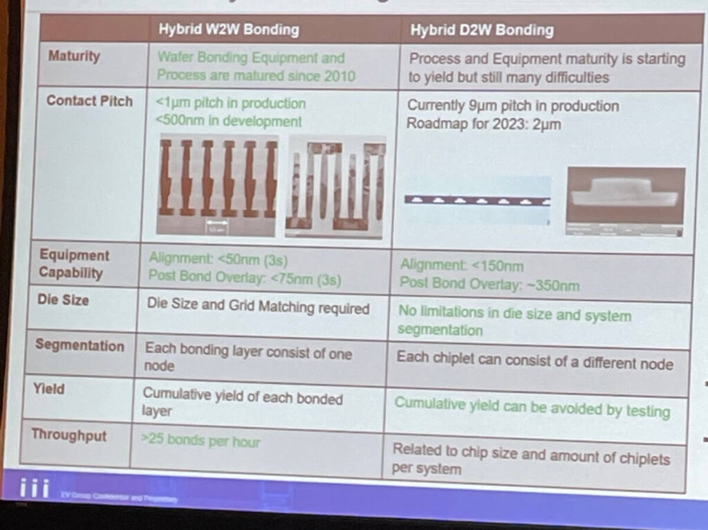
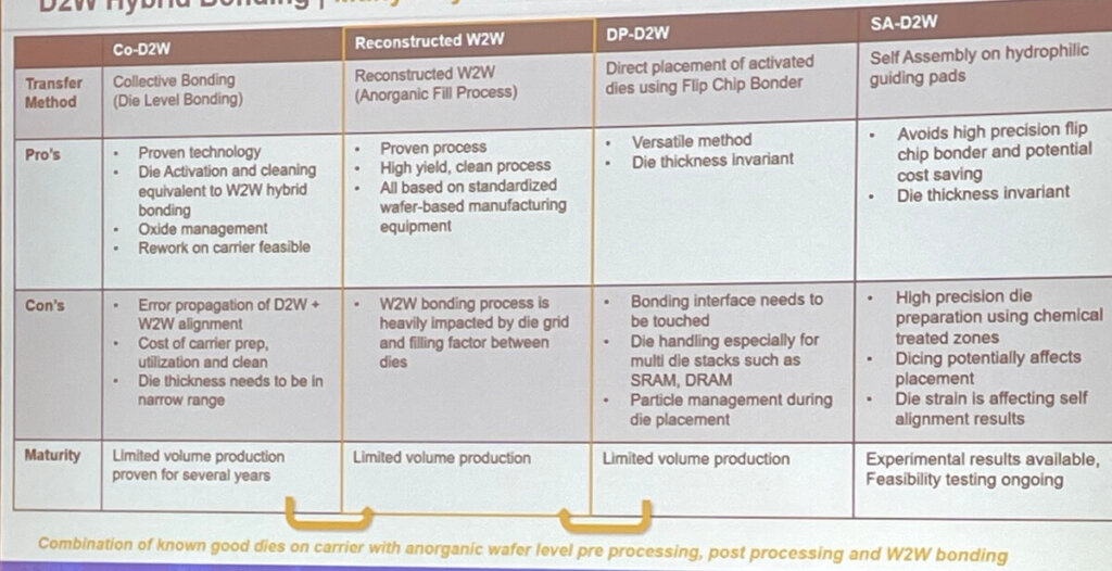
Uhrmann continued the equipment and process challenge discussion for hybrid bonding by comparing the status of D2W versus W2W hybrid bonding. (Figure 3).
He also shared a table of the many ways D2W hybrid bonding can succeed through different combinations of known-good dies on carrier with inorganic wafer level pre-processing, post-processing, and W2W bonding (Figure 4).
You can learn more about what’s happening in the world of hybrid bonding in an upcoming episode of the 3D InCites podcast featuring interviews with some of the folks who pioneered hybrid bonding: Laura Mirkarimi and Abul Nuruzzaman, Adeia. Additionally, I interviewed the EV Group team; Emilie Bourjot of CEA Leti, who presented a novel D2W process at ECTC; and Monita Pau, Onto Innovation, who provides the metrology perspective. That episode will drop on June 29, so mark your calendars or just follow along here.
CHIPS and Science Act Update
The CHIPS and Science Act was signed into law on August 22, 2022, and since then government and the microelectronics industry have been collaborating to sort out just what is needed and where the funds should go. ECTC 2023 hosted two-panel sessions – one as part of the HIR Workshop and the other organized by Nancy Stoffel, Jan Vardaman, and Bill Chen. Additionally, this year’s Diversity and Career Growth panel, organized in collaboration with iTHERM, focused on diversifying our technical workforce to meet national needs, including the CHIPS Act Initiative.
Top of mind for everyone was how the CHIPS Act funds —which is earmarked at $39B for incentives and $11B for R&D (including advanced packaging) — will help bring advanced packaging to North America, and where the workforce to support these efforts will come from.
There are many working parts that need to come together – and outreach is happening across government agencies including the National Science and Technology Council (NSTC), National Institute for Science and Technology (NIST), DARPA – which did not receive CHIPS Funding for its Electronics Resurgence Initiative (ERI) – and others.
To make sense of all of this, I invited the panelists to sit down with me for a podcast interview to discuss the takeaways. That interview will be featured in Thursday’s episode, along with the keynote interview, and an interview with Brewer Science’s Kim Yess, who was on the organizing committee for this year’s Diversity and Growth panel. You can follow the 3D InCites Podcast on Apple Podcasts, Spotify, Amazon, Google, or wherever you get your podcasts.


