StratEdge has been designing and manufacturing packages for high-power, high-frequency compound semiconductors since the early 1990s, with much attention focused on gallium arsenide (GaAs) and gallium nitride (GaN). Because of its ability to operate at very high currents and high voltages, gallium nitride GaN is widely used in applications for high-power devices operating at high frequencies.
While much attention is given to GaN devices, what is often overlooked is the package in which the GaN device is attached and the way the device is attached to the package. It’s well known that GaN device efficiency and reliability can be improved by creating a package environment that reduces chip-to-package junction temperatures (TJ).
GaN devices, especially GaN on silicon carbide (SiC) devices, can handle higher temperatures allowing designers to make circuits smaller. The GaN chip can produce much greater power density, but it becomes the package’s job to help remove the heat that is generated. The goal is to increase the power output that a device can achieve, thereby maximizing its performance. Therefore, it is important to provide the most efficient way to dissipate the heat so the device isn’t as likely to overheat and fail from normal operation.
The challenge is finding a suitable package for GaN because of its extremely high power density. What makes the package more suitable is a heat-spreading base made with a high thermally conductive material. The epoxy or solder material used to mount the GaN device onto the base is also important since the heat generated by the device must pass through this layer.
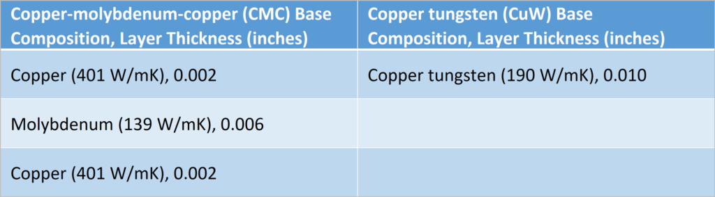
The thermal conductivity of the base material is not the only consideration. Its coefficient of thermal expansion (CTE) is also critical. The high temperatures produced by GaN require a base with high thermal conductivity and a CTE matched to the GaN device. Engineered materials like copper tungsten (CuW) composite and laminated copper-molybdenum-copper (CMC) were developed within the industry to construct robust packages.
While copper is an excellent heat conductor with a thermal conductivity of about 400 W/mK, it expands greatly when it becomes hot compared to the GaN device. Bases made with CuW composites combine the desirable thermal conductivity of the copper with the stiffness provided by the tungsten, but experimentation found that bases made with laminated layers of copper and molybdenum proved to be the best fit for GaN. Molybdenum, while not a great thermal conductor, is stiff and can be laminated to copper to provide a core that enables the entire base to have a good CTE match with the GaN device. CMC, constructed with a 1:3:1 ratio, results in an optimum balance of thermal dissipation and expansion match for the base material. The effective thermal conductivity in the z-direction is close to that of CuW, which is about 190 W/mK. What CMC provides that CuW does not is a layer of copper directly beneath the GaN device. This enables the heat to spread away from the hot spots on the bottom of the device, which helps reduce the TJ.
StratEdge recently conducted a series of thermal simulations to compare how well heat is dissipated from a GaN device. This article explains the boundary conditions of the simulations and presents the results using various die attach and base materials.
For this study, materials were used that have CTEs known to match that of GaN-on-SiC; therefore, the effects of potential mismatches are not discussed. So too for the die-attach materials. The modulus of elasticity of solder alloy versus organic polymers can be important as are many other factors, but the focus of this study is on heat transfer and the TJ of the device. The TJ is the highest operating temperature of the bottom of the GaN device in the package. As mentioned above, the TJ has a direct correlation to reliability; the lower the TJ, the longer the device lasts.
We will compare two different base materials, CuW (15% Cu/85% W), and CMC, to determine the effect they have on TJ, all other things being equal (Figure 1).
We then compare gold-tin (AuSn) solder alloy to a traditional silver-filled epoxy (H20E) (Figure 2).
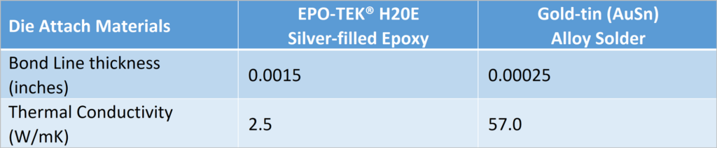
There are different methods for AuSn die attach. StratEdge chose scrubbing, which is the process of heating with mechanical agitation. It’s the extremely thin bond line, which can only be achieved with the scrubbing process, that optimizes heat transfer and results in a near void-free attachment. In addition to providing superior thermal performance, AuSn solder can be used for high-reliability applications because it won’t outgas, and it is unlikely to fail if done properly.

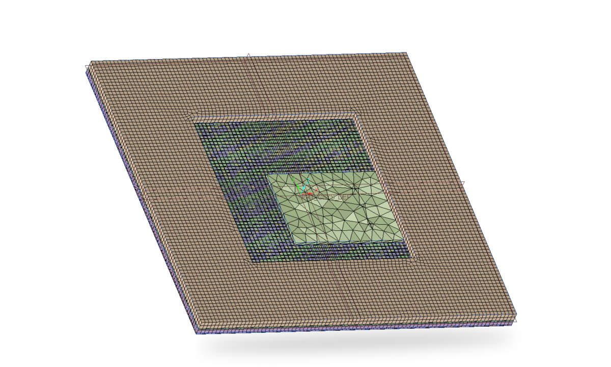
GaN MMIC and Package Simulation Model
The device used in the model is a 10-watt high-power GaN MMIC with three output stages. It is 0.1498” in length from RF-in to RF-out and 0.1134” wide. The output stages are evenly spaced 0.0375” from the output end of the device and each generates 3.333 watts. The device is attached to a metal heat spreader that is the base of a ceramic package. Both the package and heat spreader are 0.450” square in size. The metal base is 0.010” thick. The device is 0.004” thick.
To perform the steady-state thermal analysis, a model was created that mirrored the packaged device assembly ( Feature Image). As in the actual assembly, the device is offset from the center of the package. The package used was an off-the-shelf StratEdge Leaded Laminate (LL) Series package, part number LL4545-0-2, with broadband RF performance from DC to 63 GHz. The device’s RF output port was aligned next to an RF pad on the package as close as possible to the cavity wall so that the ribbon connecting the device to the package was as short as possible. StratEdge packages are manufactured with essentially no braze fillet, which allows the device to be mounted practically touching the ceramic cavity wall at the output side of the package.
The simulation software used was PTC CREO developed for use with Ansys. The boundary conditions for the model were a 0.00025” wide border within the perimeter set at a constant 75°C. The 10 watts generated by the device were divided equally over the three output stages. Each stage was 0.00039” wide by 0.00087” long. The software program allowed each stage to be divided into eight 0.00015” square elements with 0.00009” spacing between them.
Comparisons of CuW to CMC and Silver-Filled Conductive Epoxy to AuSn Solder
Using the above model, the peak output stage temperature of the device attached using H20E on a base made from CuW (15% copper) was compared to the same mounted on a CMC base. Refer to Figure 2 for all bond line thicknesses. The TJ for the model with the CMC base was 272.9°C, which was 8.9°C cooler than the model with the CuW base. Then the model with the CuW base and H20E die attach material was compared to the same base with AuSn solder die attach material. The TJ for the model with AuSn was 257.3°C, which was 24.5°C cooler than the model with the H20E. When the model for die attached to CuW with H20E was compared to CMC attached with AuSn, the TJ dropped to 247.3°C, which was 34.5°C cooler. The simulation indicates that the device mounted onto a CMC base using AuSn with a bond layer of about 0.00025” runs at a significantly cooler temperature than the device mounted on an industry-standard base material with die-attach epoxy.
The results were consistent with those reported by an independent party who made thermal measurements of a similar high-power GaN amplifier assembled under the same two configurations.
Summary and Conclusions
To quantify the benefit of mounting GaN devices with AuSn solder with ultra-thin bond lines into a package with a CMC base, a model was created for a 10-watt high-power GaN MMIC. The simulation showed that attaching this device to CuW using H20E created a TJ that was 34.5°C hotter at the hottest junction for the same device mounted on CMC with AuSn. Measured verification of the study results is in process but not yet available. Using StratEdge’s proprietary eutectic die attach method to attach a GaN chip to a StratEdge LL Series package made an amazing difference. By using packages with CMC bases and the AuSn eutectic die attach method that uses mechanical agitation and heat, chip temperatures are reduced, which improves the efficiency and reliability of the device.
Erik Sanchez also contributed to this article.
This article originally appeared in the 2024 3D InCites Yearbook. Read the issue here.