2024 3D InCites Technology Enablement Awards Finalists
For the 2024 3D InCites Awards, we decided to change things up a bit and do away with our standard categories from previous years. Instead, we will be awarding five Technology Enablement Awards to companies who have identified a challenge in the adoption of Heterogeneous Integration (HI) 3D HI, and chiplet architectures, and developed a viable solution to address it.
Our advisory board reviewed applications and has selected the following eight, 2024 3D InCites Technology Enablement Awards finalists. Each applicant answered three questions: What is the challenge you’ve identified, what is your solution, and how does it apply to the commercialization and manufacturing of HI, 3D HI, and chiplets? What follows are summaries of how each finalist answered these questions.
DECA
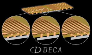
The semiconductor industry is transitioning from silicon interposers to molded fan-out interposers with embedded bridge die for progressively larger devices. As highlighted in TSMC’s keynote at IMAPS San Diego in October ’23, precisely aligning embedded bridge dies presents a substantial manufacturing challenge that leads to potential risk of yield loss, particularly as devices become more intricate.
In response to this manufacturing challenge, DECA has unveiled a groundbreaking solution known as Adaptive Pad Stacks. This innovation signifies a significant leap forward, delivering an order-of-magnitude increase in the allowable die shift for embedded bridge die in molded fan-out interposers. The resulting enhancement in manufacturing tolerance not only safeguards against yield losses but also facilitates the highest density interconnect on more complex devices, including cutting-edge AI processor applications. When integrated with proven technologies such as Adaptive Alignment, Adaptive Routing, and Adaptive Metal Fill, Adaptive Pad Stacks provides a robust and comprehensive solution for foundries, OSATs, IDMs, and other industry players involved in designing and producing the most advanced HI chiplet assemblies of the future.
ERS Electronic GmbH
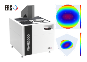
Wafer and package warpages pose a significant challenge for the widespread adoption of HI, 3D HI, and Chiplet-based architectures. Thermal mismatch among different materials exacerbates this issue, potentially leading to misalignment of interconnects, reduced bonding efficiency, and long-term reliability concerns. Even minimal warpages in these advanced architectures can result in signal integrity issues and degraded performance. Addressing this challenge requires multidisciplinary efforts in material engineering, including substrates with low coefficient of thermal expansion (CTE), underfill materials, process optimization, and advanced metrology tools for real-time monitoring during manufacturing.
To address wafer and package warpage, ERS Electronic GmbH developed the Warpage Measurement System Wave3000. This in-line metrology system accurately measures wafer warpage using advanced optical sensors, identifying risks before proceeding to subsequent processing steps. The Wave3000 can be integrated at various points in the manufacturing line, ensuring continuous monitoring and mitigation, to address warpage caused by integrating multiple materials with varying CTE. With its data-driven approach, the system provides crucial information ahead of time, enabling dynamic adjustments to process parameters and preventing the risk of sending warped wafers that subsequent machines may struggle to handle, ensuring mass production and commercial viability of HI, 3DHI, and Chiplets.
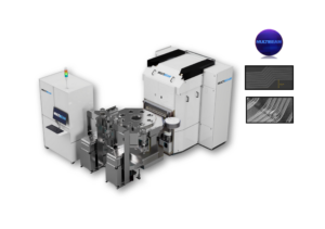
LPKF Laser & Electronics SE – Laser-Induced Deep Etching
Glass substrates are becoming a viable alternative to silicon for HI, 3DHI, and chiplets. However, there are challenges with cost-effectively achieving precise and reliable through-glass vias (TGVs) and other microstructures using traditional drilling methods. Fabricating high-quality, high-density, and small-diameter TGV patterns in glass, without causing damage or stress, is paramount to realizing optimal device performance, achieving miniaturization, and ensuring cost efficiency and yield.
To address this challenge, LPKF Laser and Electronics developed its Laser-induced deep etching (LIDE) technology. Using a non-ablative, single-pulse laser-based process, it’s possible to achieve high aspect ratio, high-density TGV arrays without stress or microcracks. LIDE is ultra-fast and can create multiple structures in one step. It’s also compatible with a range of glass types, including thin and ultra-thin substrates.
LIDE technology is said to be highly scalable and suitable for mass production. Its promise of rapidly and reliably producing high-quality glass microstructures positions LPKF as a key enabler in the commercialization and manufacturing of next-generation HI, 3DHI, and chiplet-based devices.

Multibeam Corporation
The semiconductor industry faces a challenge as chip-to-chip interconnect scaling lags behind on-chip scaling, creating a bottleneck in system performance. Advanced packaging’s role in improving system performance is hindered by limitations such as beachfront I/O density, die integration issues, and difficulties in achieving high-bandwidth chip-to-chip interconnects, mainly due to variations in chip thickness and die placement accuracy. Patterning system constraints compound these challenges, affecting multi-die integration. The slow cycle times of mask-based lithography technologies contribute to development delays in the Heterogeneous Integration Roadmap (HIR).
Multibeam addresses these issues with its Multi-Column E-beam lithography (MEBL) solution. This maskless technology enhances multi-die integration with a large write field, high DoF, ultra-fine resolution, and adaptable writing, supporting diverse components on a single substrate for AI applications. MEBL makes it possible to pattern more than 10X larger than current interposers, facilitating wafer-scale integration for processors like HPC, GPUs, and AI engines. With more than 100X DoF improvement over optical lithography, it enables advanced 3D structures and high-resolution interconnects, resulting in a 10x-100x increase in chip-to-chip interconnect bandwidth. This technology expedites in-package data analysis, inference, and decision-making with low power and low latency, promising breakthroughs in chips-first and chips-last packaging and on-wafer extended integration.
Multibeam’s technology accelerates time-to-market for multi-die packages and overcomes throughput limitations. Its scalable modular architecture allows for seamless transitions from pilot to production. Its adaptable and extendable patterning capabilities and the ability to customize substrates and implement design changes without masks position this technology to drive advancements in silicon integration for future generations.
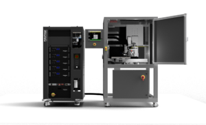
PulseForge, Inc.
Fabricating 3D ICs involves stacking thinned silicon (Si) wafers and vertically interconnecting them using through-silicon vias (TSV). To handle thinned Si wafers, temporary bonding to a rigid carrier is required before thinning. The crucial step of wafer debonding, separating the thinned wafer from the carrier, is typically done using chemical solvents, mechanical means, or heating the adhesive. Laser-assisted wafer debonding is an attractive alternative, leveraging optical energy to promote adhesion loss at room temperature. However, challenges like beam width limitations necessitate exploring alternative high-throughput debonding techniques.
Photonic Debonding (PDB) utilizes high-intensity light pulses and a proprietary inorganic light-absorbing layer to separate temporarily bonded wafer pairs efficiently. This technology offers a cost-effective alternative to traditional laser techniques, providing benefits such as lower processing costs, minimal thermal impact, reduced mechanical strain, and ash-free debonding. Operating at room temperature, PDB is particularly advantageous for advanced packaging applications, enabling efficient debonding of ultra-thin wafers during back-end-of-line processing with increased final device yield.
To bring PDB to market quickly, PulseForge formed strategic partnerships with material suppliers and integrators in the temporary bonding/debonding infrastructure. This collaborative approach not only opens new markets and introduces the technology to customers but also validates it and gains support from multiple stakeholders. The company offers a three-tiered approach: a flexible R&D tool for fundamental research, a semi-automated debond tool for limited production, and a fully automated debond tool for fabs as a drop-in replacement for existing equipment. An extensive patent portfolio has also been developed around the equipment and the PDB process.
light pulses and proprietary light-absorbing layer coated carriers.
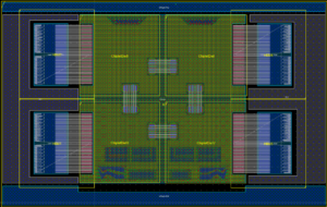
Siemens DISW
The semiconductor industry faces a challenge in adapting to the megatrend of chiplet integration for high-performance computing. Early design planning involves optimizing pin layouts for power, performance, and area, particularly in high pin count ASICs/FPGAs. These are broken down into smaller blocks, forming the complete floor plan over time. Hierarchy in design helps manage complexity by breaking structures into smaller building blocks. Parameterized representation is crucial, especially in die-to-die signal interfaces and power distribution networks within IC packaging.
Siemens uses hierarchical device modeling methods to enhance its package prototyping and planning design tool, Xpedition Substrate Integrator (XSI). This innovative set of functions and capabilities facilitates quick and comprehensive updates to design structures consisting of hierarchical building blocks or parameterized pin regions. In contrast to non-graphical IC package floor-planning flows that rely on macro-driven spreadsheets, Siemens’ approach minimizes time consumption and reduces the risk of errors during design updates.
While non-graphical floor-planning flows can generate an initial draft, keeping up with changes needed for early design analysis could be more practical. Demonstrating the efficiency of an HBM die-to-die building block with parameterized pin regions, this approach enables quick and efficient package design creation. Notably, effective hierarchy incorporation achieves iterative updates in minutes or seconds. Integrating hierarchical device planning with parameterized pin regions in the xSI design tool offers a revolutionary methodology, significantly reducing design cycle time to meet performance, power, area, and cost (PPAC) goals.
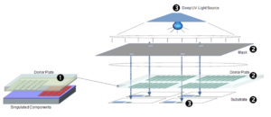
Terecircuits
Current advanced packaging techniques, such as 3D stacking, HI, and die-on-wafer, introduce complexity and additional process steps, impacting yield and slowing down throughput. To overcome these challenges and unlock the potential of advanced packaging and assembly for complex devices, Terecircuits founders envision their foundational chemistry and processes becoming the industry standard, particularly for semiconductor and display back-end manufacturing.
Traditional pick-and-place tools struggle with assembling large numbers of microscopic components, hindering the development of next-gen displays, wearables, and medical devices.
Terecircuits addresses this challenge by proposing a shift from slow and inefficient mechanical processes to a fast, controllable chemical approach.
Terecircuits’ efficient Laser-Induced Forward Transfer (LIFT) technique, powered by a new photopolymer class, delivers a cost-effective, high-yielding 10-10,000x throughput improvement. The applications span from mass transferring MicroLEDs for displays to the non-destructive transfer of delicate materials like Silicon Carbide (SiC), and stress-free assembly of thinned die for 3D stacking and flexible hybrid electronics.
Drawing inspiration from the semiconductor industry’s success in using light and chemistry for modern integrated circuits, Terecircuits aims to revolutionize the $200 billion assembly and packaging industry, offering a radical solution for assembling individual microscopic components efficiently.
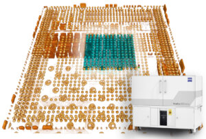
Carl Zeiss Microscopy
Complexities in 3D HI architectures are slowing down traditional package analysis, impacting success rates and extending development cycles. The limitations of X-ray microscopes (XRM) with field of view (FOV) constraints make fault isolation challenging in large IC packages, resulting in a time-consuming imaging process.
ZEISS revolutionizes 3D X-ray microscopy with AI-powered solutions for non-destructive imaging. DeepRecon Pro enhances imaging in advanced 3D packages, providing superior quality and over 4x faster data acquisition. Meanwhile, DeepScout, also AI-enabled, achieves up to 5x higher resolution for extensive FOV imaging through a deep-learning algorithm.
ZEISS’s AI-powered DeepRecon Pro enhances thermocompression bonding (TCB) processes in 2.5 and 3D packages, reducing scan times for assessing alignments and accelerating process development cycles. DeepScout extends high-resolution 3D X-ray imaging benefits to reliability testing, construction analysis, and reverse engineering applications.
Congratulations to all our Technology Enablement Award Finalists! After a final round of questions, winners will be selected and announced on February 5, 2024. The 3D InCites Awards Ceremony takes place on March 21, 2024, following the morning keynote session at the IMAPS Device Packaging Conference.