
Carl Zeiss Microscopy News

ZEISS Microscopy Showcases AI-Powered Failure Analysis
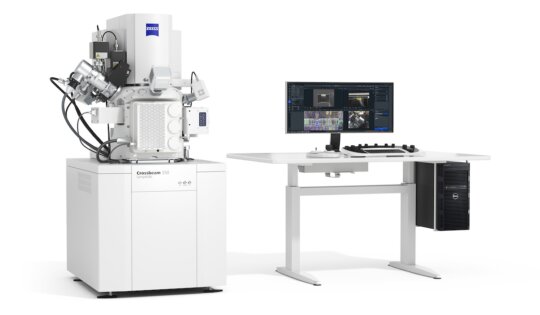
ZEISS announces involvement at 50th Annual ISTFA Conference Preview of new focused ion beam scanning electron microscopy (FIB-SEM) solutions Virtual...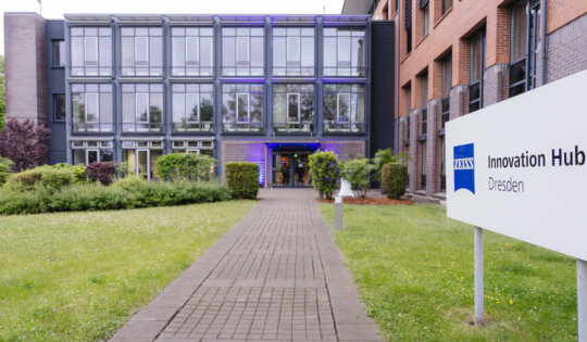
ZEISS Microscopy Opens Semiconductor Applications Laboratory in Dresden
State-of-the-art innovation lab pushes the limits of advanced semiconductor applications ZEISS has announced it recently opened the ZEISS Microscopy semiconductor...
ZEISS Adds Advanced Reconstruction Intelligence to 3D Non-destructive X-ray Imaging for Improved Semiconductor Package Failure Analysis
New iterative and deep learning reconstruction algorithms significantly enhance throughput and image quality for ZEISS Xradia Versa and Context microCT...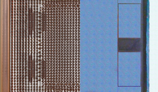
Digital Cross-section Technology for Inspecting and Measuring Buried Package Interconnects
Much has been written about the end of Dennard Scaling, the slowdown of Moore’s Law and the impact that these...
ZEISS Semiconductor Mask Solutions Receives Intel’s Preferred Quality Supplier Award
Jena, Germany, March 5, 2020 — ZEISS Semiconductor Mask Solutions has been recognized by Intel as a recipient of a...