
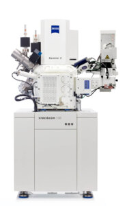
Pleasanton, Calif., and Oberkochen, Germany, February 4, 2020 — ZEISS today introduced the ZEISS Crossbeam Laser — a new family of site-specific focused ion beam scanning electron microscope (FIB-SEM) solutions that accelerate package failure analysis and process optimization for advanced semiconductor packages. Integrating a femtosecond laser for speed, a gallium ion (Ga+) beam for accuracy, and SEM for nanoscale-resolution imaging, the ZEISS Crossbeam Laser family provides package engineers and failure analysts with the fastest cross-section solution at the highest imaging performance, while providing minimal sample damage.
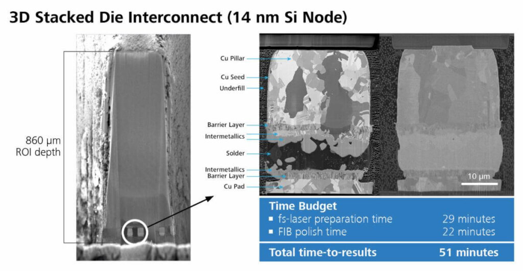
With its unique architecture, the ZEISS Crossbeam Laser family can rapidly cross-section deeply buried package interconnects such as Cu-pillar solder bumps and through-silicon vias (TSVs), as well as device back-end-of-line (BEOL) and front-end-of-line (FEOL) structures, in minutes instead of the hours or days of other approaches, all while minimizing artifacts and maintaining sample quality under vacuum. Besides failure analysis, the ZEISS Crossbeam Laser family enables structural analysis, construction analysis, reverse engineering, FIB tomography, and transmission electron microscopy (TEM) sample preparation. Several ZEISS Crossbeam Laser systems have already been sold to major global electronics manufacturers.
New Approaches to Root Cause Failure Analysis Needed in 3D Packaging
The demand for increased miniaturization and higher interconnect density in mobile and high-performance devices has driven an explosion of innovations that enable fine-pitch and multi-chip architectures. These designs are not only shrinking packaging interconnects but are also increasingly driving them into the third dimension. At the same time, new types of defects buried deep within these packages are arising that can affect yield and reliability, and therefore must be quickly found and eliminated.
In the failure analysis workflow, non-destructive analysis is carried out as a first step toward optimizing package processes and improving package yields. Instruments such as the ZEISS Xradia Versa 3D X-ray microscope are used to visualize defect sites non-destructively, followed by destructive physical failure analysis (PFA) techniques to determine and resolve a failure’s root cause. Today, package interconnect and silicon BEOL dimensions are crossing over each other. Mechanical cross-sections used commonly in PFA are now challenged to rapidly and accurately reach deeply buried structures and defects. In addition, the adoption of fragile materials in the silicon BEOL, such as extreme low-k dielectrics, leads to increasing numbers of cross-section-induced artifacts that are difficult to distinguish from true defects caused by chip and package interactions.
Plasma FIB (PFIB) is an alternative cross-section approach but is 10,000x slower than a femtosecond laser. It is too slow to address ablation volumes of >0.5 mm3 in practical timeframes, as required in many package FA applications. Additionally, PFIB lacks the resolution needed for the highest-quality TEM sample preparation, and it induces ribbon artifacts in carbonaceous materials that are common in semiconductor packages. Standalone laser systems offer fast ablation but can have large heat-affected zones, increasing the likelihood of damage to the region of interest and increased polishing time to remove artifacts. Lack of integration with a FIB-SEM makes the FA workflow slower and less efficient while risking oxidation artifacts due to atmospheric exposure prior to analysis.
“The packaging world has reached an inflection point where densities are approaching a million I/Os on a single silicon interposer, shrinking interconnects are starting to mirror the wafer fab and stacking is everywhere — in the device itself, among the package layers and within the printed circuit board. This makes fault isolation and failure analysis so much harder when a part fails,” stated Raj Jammy, Head of ZEISS Process Control Solutions (PCS) and Carl Zeiss SMT, Inc. “The ZEISS Crossbeam Laser family is designed to alleviate this pressure on the FA engineer, providing revolutionary time to results using a best-of-breed approach that combines speed, accuracy and high-resolution imaging all in a single instrument.”

The ZEISS Crossbeam Laser family offers an optimal PFA solution that dramatically improves total time to results while providing the highest imaging performance. Features include:
Femtosecond laser for large volume removal with minimal artifacts (up to one cubic millimeter of silicon in only 30 minutes versus hours or days with other methods)
ZEISS’s Gemini optics, which provide the highest image quality and analytics
Ga+ FIB, which provides high-speed milling with 100nA combined with 500V fine polishing to reduce amorphization
Accurate localized end pointing using FIB resolution (down to 3nm)
Isolated laser chamber to segregate ablation contaminants from the main imaging chamber and maintain the highest-resolution imaging capability while keeping maintenance costs low
Easy sample transfers between the FIB-SEM and laser chambers without breaking vacuum
Laser preparation is suitable for many materials, including silicon carbide and glass
The ZEISS Crossbeam Laser combined with the ZEISS Xradia Versa XRM provides a powerful addition to standard FA workflows that will enable higher FA success rates and accelerated time to problem resolution.
For more information on the ZEISS Crossbeam Laser family, please visit: www.zeiss.com/pcs
Press contact
Victoria Doll
ZEISS Process Control Solutions
Email: info.pcs@zeiss.com


