
Much has been written about the end of Dennard Scaling, the slowdown of Moore’s Law and the impact that these events will have on future semiconductor performance and technologies.[1] Much has also been written about semiconductor performance improvements that advanced IC packages are expected to provide that previously resulted from silicon scaling.[2] However, these packaging improvements depend on one primary factor — the ability to shrink package-level interconnect size and density on a scale that has never been done before.
Why Do We Need Cross-sectioning?
Although package technologies have evolved significantly since dual in-line and C4 flip-chip packages were developed, minimum package interconnect feature sizes have not scaled significantly over the past 40 years. Just to put this into perspective, minimum silicon critical dimensions have scaled by nearly 10,000:1 during this period[3] while minimum package interconnect size has scaled by less than 10:1[4].
The ability to scale package interconnects is in turn dependent on two factors:
- The ability of the manufacturing processes to fabricate the desired interconnect structures while maintaining acceptable levels of quality and process variation
- The ability to accurately set up and monitor the results of these manufacturing processes in a timely manner
While it is beyond the scope of this article to assess the viability of the various package manufacturing processes to fabricate the desired structures, manufacturing process setup and results monitoring are separate and equally challenging requirements and are the subject of this work.
Except for wire bonds, most internal package interconnects cannot be viewed either during or after the assembly process. As a result, physical cross-sections are often the only available method for verifying the internal results of process setups and production builds. However, physical cross-sections are destructive, take a long time to process, provide a limited field-of-view, are limited to two dimensions and are highly operator-dependent.
Fortunately, an innovative, non-destructive alternative to physical cross-sections is available called “digital cross-sectioning”. Digital cross-section technology can replace most physical cross-section approaches used for assembly process setup and construction analysis and can also be used in circumstances where products are “blind-built” without physical verification.
Digital Cross-section Technology
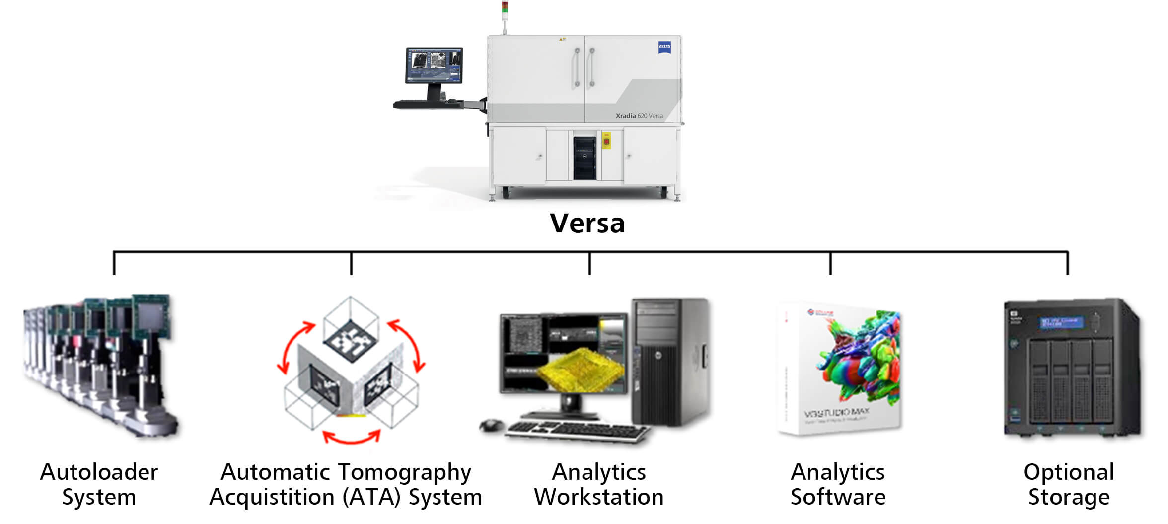
Digital cross-section technology is available from ZEISS with the RepScan® system, which is based on the company’s Versa 3D X-ray microscope with Resolution at a Distance™ and spatial resolution of 1 µm at 50 mm working distance, along with additional custom hardware and software as shown in Figure 1. The RepScan system can image and measure the following package features:
- Interconnect bond line and die tilt
- Bump-to-pad and through silicon via (TSV)-to-bump alignment
- Solder fillet extrusion, solder volume, and solder wetting
- Internal layer warpage and other X-ray imageable features

Figure 1: ZEISS Versa RepScan system.
In the following sections, we will demonstrate process setup and construction analysis data that was extracted non-destructively from a fully assembled 2.5D package using this digital cross-sectioning system.
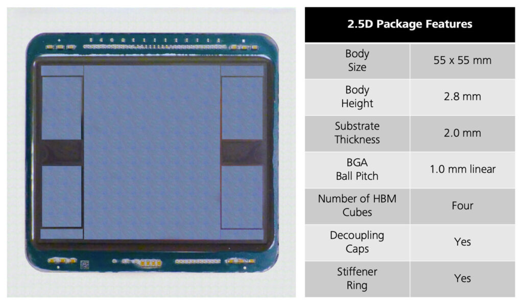
A typical 2.5D package consists of four high bandwidth memory (HBM) cubes and a central processing unit (CPU) mounted on a silicon interposer, which is in turn mounted on an organic substrate:
- HBM cube – Consists of four to eight memory chips assembled on a logic chip and electrically connected using TSVs and micro-bumps. The HBM cube is a purchased part and is almost always assembled and tested in a different factory from the 2.5D package.
- 5D interposer – The process flow referenced in this article utilizes pre-stacking of the HBM and CPU on the 2.5D interposer before assembly to the organic substrate. The pre-stacked system is encapsulated with resin before being assembled on the substrate. An alternative assembly flow is to assemble the 2.5D interposer to the organic substrate before connecting the chips.
- Organic substrate – The pre-stacked 2.5D chip module is then assembled to the organic substrate using C4-type bumps and underfilled. Decoupling capacitors, stiffener rings, and heat spreaders might also be assembled on the substrate, depending on the application.
The 2.5D package used in this analysis is typical of many current designs and is shown in Figure 2.
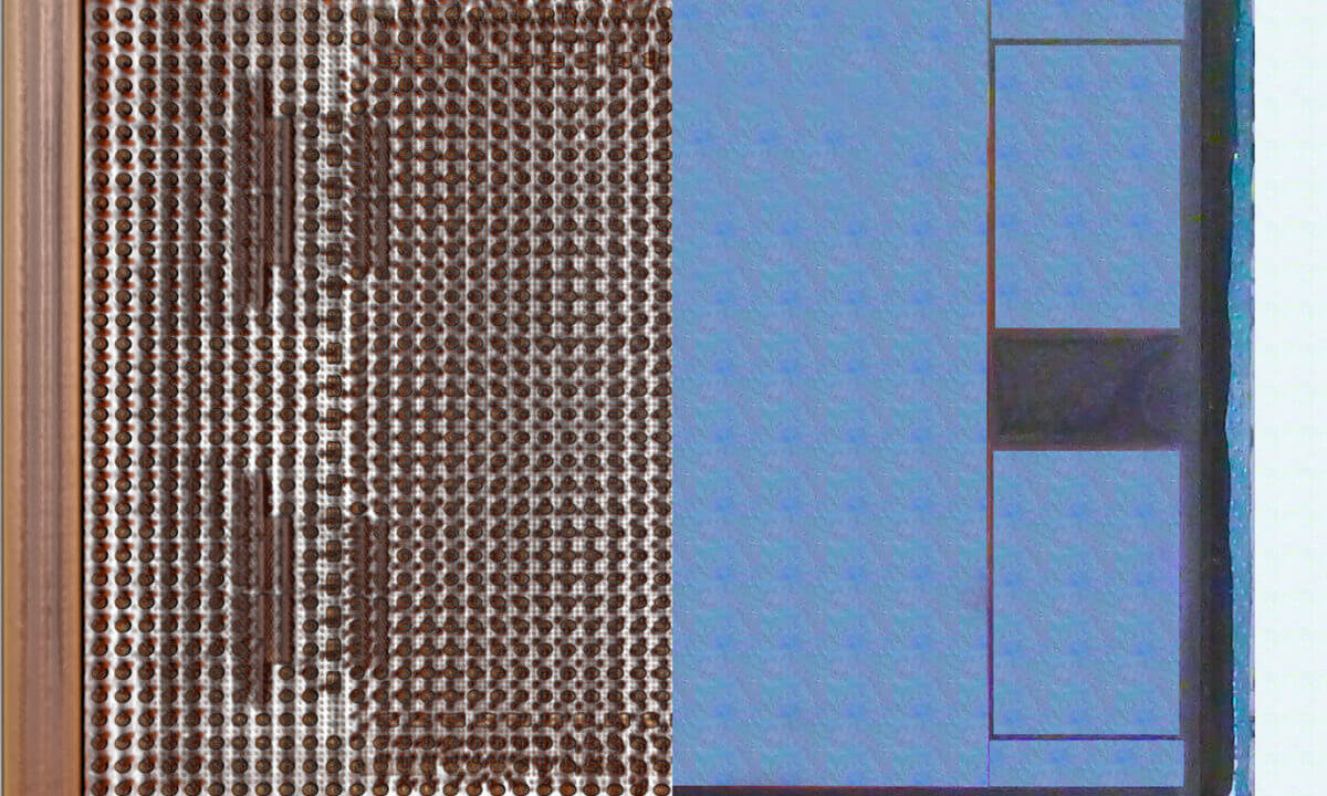
As previously mentioned, the HBM cube is a purchased part for the 2.5D manufacturer. While the external electrical interface to the HBM cube and overall stack height are defined by a JEDEC specification[5], the horizontal stack outline, internal electrical interconnects, and stack configuration are unique to each memory supplier. While it is relatively uncommon for a 2.5D customer to do construction analysis of an HBM cube, we have included this analysis to demonstrate the capabilities of the RepScan 3D X-ray digital cross-sectioning system.
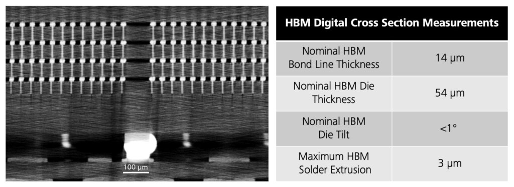
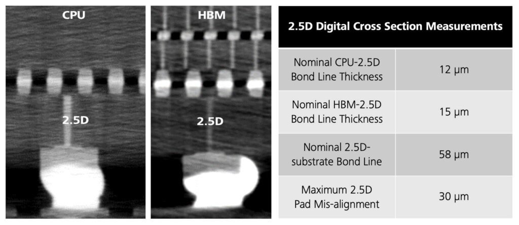
Because of the thinness of the memory chips and the small size of the micro-bumps, thermo-compression bonding is almost always used for HBM assembly. Figure 3 shows an image and a small sample of the characterization data that can be extracted from the HBM stack using the digital cross sectioning technique.
The assembly flow for this package uses pre-stacking of the HBM modules and CPU on the 2.5D interposer prior to assembly on the organic substrate. The pre-stacked chipset and 2.5D interposer are encapsulated and bumped before being assembled onto the organic substrate. Figure 4 shows images and a small sample of the characterization data that can be extracted from the pre-stacked chipset using the digital cross-sectioning technique.
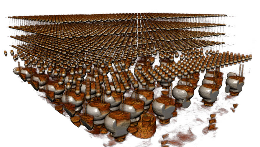
After encapsulation and C4 bumping, the pre-stacked 2.5D chip module is singulated and assembled to the organic substrate using mass reflow and then underfilled. Decoupling capacitors, stiffener rings, and heat spreaders might be assembled to the substrate at this time as well. At this point, the 2.5D package is complete and ready for electrical testing. Figure 5 shows a 3D rendering of the interconnects in the finished 2.5D package.
Conclusion
In this analysis, we have demonstrated a small fraction of the measurements that can be extracted from a fully-assembled 2.5D package using the digital cross-section technique. Image quality and measurement results would be improved significantly if the technique were used when the package is partially assembled.

Editor’s Note: This article first appeared in the 3D InCites Yearbook. Download your copy here.
References
[1] John L. Hennessy, David A. Patterson, “A New Golden Age for Computer Architecture.” Communications of the ACM, February 2019, vol. 62 no. 2, pp. 48-60
[2] Mark Lapedus, “Planning for Panel-Level Fan-Out”, Semiconductor Engineering, November 2019, https://semiengineering.com/planning-for-panel-level-fan-out/
[3] Mehrdad Shaygan, “Why Nanoelectronics is better than Microelectronics?” SPINOGRAPH, May 2016, http://www.spinograph.org/blog/why-nanoelectronics-better-microelectronics
[4] Mikhail R. B et al., “Advanced Interconnects: Materials, Processing, and Reliability”, ECS Journal of Solid State Science and Technology, 2015 volume 4, issue 1, Y1-Y4, doi: 10.1149/2.0271501jss
[5] JESD235 High Bandwidth Memory (HBM) DRAM standard. JEDEC Solid State Technology Association, Nov 2018, pp.115-116
About the Authors
Thomas Gregorich is Director of Business Development at ZEISS Semiconductor Manufacturing Technology where he is responsible for products marketed by the Process Control Solutions Business Unit for advanced packaging. Previously Mr. Gregorich held senior-level positions at Western Digital, Micron, Broadcom, MediaTek and Qualcomm. Prior to his position at Qualcomm, Mr. Gregorich worked for Motorola and had assignments in the United States as well as Japan, Taiwan and China. Mr. Gregorich has a BS in Mechanical Engineering from Bradley University, an MBA from Northern Illinois University and is a Senior Member of IEEE.
Edith Hu works as Market Research Analyst at ZEISS Semiconductor Manufacturing Technology Process Control Solution SBU. She actively collects and analyzes industry news to understand the market landscape. Ms. Hu also works on strategic marketing for products in Failure Analysis and Advanced Packaging spectrum. She worked as Data Analyst before joining ZEISS. Ms. Hu has MS in Innovation and Management from Tufts University, and BS in Finance from East China Normal University.
Masako Terada is an experienced application engineer with a demonstrated history of working in 3D X-ray microscopy and image visualization and analysis field. Since joining ZEISS PCS in October 2018, Ms. Terada has been responsible for providing technical details to support sales and marketing activities, getting involved in new product launch, and training customers around the globe. She has enjoyed working with customers, students, and researchers visualizing and analyzing many different types of samples in academia and industry over more than 15 years.


