
Advanced packaging (AP) processes are often described as the front-end-like processes that have migrated to traditionally back-end applications for packaging semiconductor devices. However, AP processes also draw on techniques developed in the other direction, downstream from packaging at the assembly level, where packaged devices are connected to each other on printed circuit boards (PCB), typically using surface mount technologies (SMT). Just as features are scaled up from their front-end sizes to connect devices in AP processes, they are scaled down from the SMT/PCB world, ultimately comprising a size range from about 10µm to 100µm that has been called the “middle-end”.
Many of the techniques used in SMT, especially inspection and measurement, can be scaled successfully for AP applications. The evolution of high-resolution, phase shift profilometry (PSP) is one example. The technique’s ability to provide fast, accurate, 3-dimensional characterization has earned it a central role in SMT processes. Now, the latest generation of sensors (Nano Resolution MRS™, CyberOptics Corporation )provides nanoscale sensitivity to height variation and micrometer-scale spatial resolution at production-worthy speeds that are significantly faster than alternative technologies.
In adapting PSP technology to AP sensors, engineers were challenged to increase the resolution of the optical system while preserving the technique’s high speed. Another, less obvious, hurdle was the need to measure specularly reflective surfaces, such as solder bumps, for which accurate 3D measurements of height and coplanarity are critical. Conventional PSP technology requires a diffuse reflection from the measured surface. The new sensor includes a dedicated channel for specular surfaces that provides fast, accurate measurements.
Phase Shift Profilometry
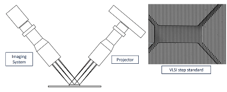
PSP uses structured light to measure the topography of a surface (figure 1). It projects a pattern of light and dark fringes onto the surface from one direction and views the surface from a different direction, looking for distortions in the pattern caused by changes in surface height. If the pattern is a series of straight, regularly spaced fringes projected from directly above the surface, and the surface is perfectly flat when viewed from a different angle the fringes will remain straight and parallel. If there are bumps or depressions in the surface, the fringes will appear to curve or shift. Knowing the difference between the projection and observation angles and measuring the direction and magnitude of the shift, we can calculate the change in surface height. Since the intensity of the fringe varies sinusoidally, we can measure exceedingly small shifts in its position. The “shift” in phase shift technique derives from shifting the sinusoidal pattern by known increments (e.g.. 90 degrees) to solve for reflectance, fringe contrast, and the phase.
The calculation becomes slightly more complicated when the surface has abrupt changes in height, such as a feature with a flat surface and vertical walls. The fringes will show discontinuous shifts where they cross such a feature. The size of the shift still indicates the difference in height, but the direction and magnitude of the shift are no longer obvious. Did the surface change up or down? Did the fringe shift half a fringe or one and a half fringes? There are ways to eliminate these ambiguities and other measurement limitations by using multiple patterns with different frequencies and orientations, and multiple cameras to view from different perspectives.
One of the great advantages of PSP is that it is an image-based technique that captures data from the full field of view simultaneously, makes it much faster than alternate technologies. Using multiple cameras viewing from different directions multiplies this advantage by capturing multiple images simultaneously. The translation of measured phase shifts into height variations, known as unwrapping, is performed by sophisticated software routines that run with extraordinary speed on modern graphic processors. In practical terms, our latest sensors can inspect the full surface of as many as twenty-five 300mm wafers per hour with 50-nanometer height resolution and 3µm spatial resolution.
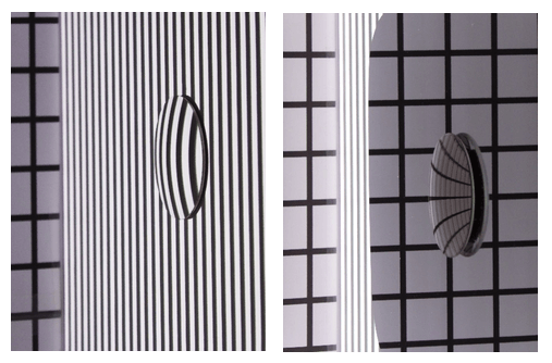
Specular Reflections for AP Processes
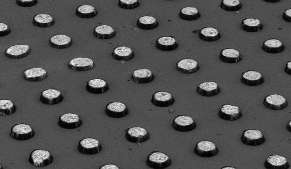
Specular (mirror-like) reflections are an example of one of the hurdles facing engineers in adapting PSP to advanced packaging applications. Specular surfaces on features like solder bumps and pillars are common and their measurement is critical to ensure the integrity and reliability of vertical connections between stacked chips or between chips and substrates.

Figures 2a and b illustrate the twofold challenge of specular surfaces for conventional PSP: 1) spurious multiple reflections between specular surfaces can introduce errors in the measurements and 2) the projected fringe pattern is not visible on a specular surface.
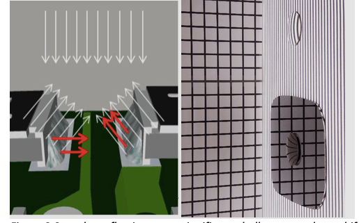
Spurious multiple reflections occur when bright light falling on one feature is specularly reflected with another feature and then back to the sensor, giving an erroneous reading of the fringe intensity for that point. Because specular reflections are highly directional, comparing images from multiple cameras provides one way to detect and eliminate their effects – they are unlikely to appear the same from different directions. Likewise, they are unlikely to appear the same when illuminated by fringe patterns with different spatial frequencies (figures 3a and b). The combination of these and other analytical techniques allows us to successfully reject spurious reflections in our MRS (multiple reflection suppression) sensors.
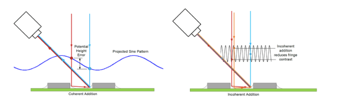
The second challenge, measuring specular surfaces, requires a different approach. Conventional PSP relies on measuring the intensity of a diffuse (non-directional) reflection from the measured surface that is representative of the intensity of the projected pattern at that point. Although we cannot see a shadow on a mirror, we can tell something about the shape of the mirror surface by analyzing its effects on the reflected image (Figure 4). In this analysis, the mirror surface is treated as an element in the optical path. Our latest generation of MRS sensors includes an additional channel dedicated to measuring specular surfaces with optical analysis of the reflected light.
To remain profitable, electronics manufacturers must continually monitor process performance to detect and correct problems and ensure yield. Inspection and metrology are the indispensable foundation of process control. In the same way that process technologies are converging in advanced packaging processes, inspection and measurement technologies are migrating from both directions, front- end and back-end, to the new middle-end. With its high speed, nanoscale resolution, ability to measure reflective surfaces, and proven track record in SMT applications, MRS technology is poised to assume a central role in AP process control.


Comments are closed.