
Technology is Key
With the ever-present pressure to produce more efficient devices with more power, the sizes of the structures and electrical connections in the production of chips have become smaller and smaller. In addition, the sheer number of these connections in a given unit area has also increased in a spectacular way. At the heart of all X-ray inspection, whether it is manual or fully automated metrology, is the imaging chain. This can be thought about in basic terms by the two main elements: The source and the detector. Over the decades these two fundamental items have had to evolve enormously to keep up with the ever-growing demands of the semiconductor industry.
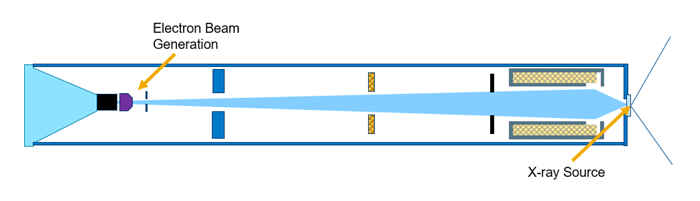
All X-ray sources are designed to balance three things: Power, resolution, and lifetime. The most advanced today is the Sealed Transmissive Tube (Figure 1). This combines high resolution, and long lifetimes at high power while producing a consistent source of X-rays. This stability, flexibility, and quality could not be more important to the inspection of such small but ever-so-important structures.
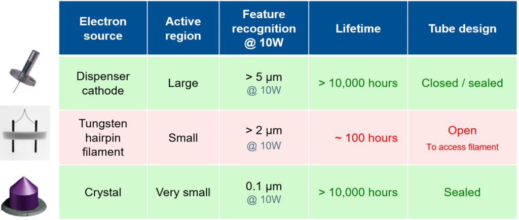
Fundamental to this design is the crystal filament which produces a very fine, efficient electron beam. This material can do this far below its critical temperature, providing a much longer life than with a Tungsten filament. When this beam hits the target material the X-rays are produced. This design allows the device under test (DUT) to be placed very close to the source of the X-rays giving the highest possible magnification. Magnification is defined by the ratio of the distance from source to object and source to detector.
Inspection Strategy Should Always be a Zero Defect Strategy
The further into the manufacturing process, the more time and expense have been invested into a single device. That can start adding up very, very quickly into 10s of 1000s of dollars.
Identifying defects early is essential, particularly as more and more devices are being used in sensitive applications such as aerospace, autonomous driving vehicles, medical devices, etc. Failure or breakdown in the real world is simply not an option. If the entertainment system breaks in a car, it’s inconvenient, but if the ABS system fails, lives depend on it. In this context, an X-ray has the task of making sure that everyone is safe.
There are several ways this can go wrong. If the electronic connections aren’t strong, they can become susceptible to early life failures through, for example, thermal cycling. Let’s look at how processors are usually used. They get really hot, they get turned off, and then they’re cold, then hot, then cold, and so on. Components and bonds can then start cracking and breaking if they don’t have a really good connection or are made of low-quality materials.
The Complete Inspection Picture
Nordson TEST & INSPECTION designs, develops and manufactures various differentiated technologies that complement each other. These include acoustic, optical, and manual X-ray inspection, autonomous X-ray inspection, X-ray component counting, semiconductor wafer metrology, semiconductor metrology sensors, and Nordson X-ray technologies.
A good example is to use both acoustic and X-ray inspection. Acoustic inspection is very strong when viewing delamination in the silicon wafers themselves, which is much more of a challenge for X-rays. If this defect is not viewed from the correct angle the imaging isn’t able to create a clear contrast between that empty space and the material around it. But when the sound wave in acoustic imaging hits this air gap it cannot pass through, is reflected back and detected, giving the strongest signal possible. Conversely, where it is difficult to get this acoustic signal back or detect it transmissively (due to scattering or obstruction by another void), X-ray makes inspection simple.
In a similar way, 2D X-ray imaging is complimented by 3D inspection, allowing users to analyze in ever greater detail.
This is done using computed tomography (or CT), which provides the ability to create 3D models that can then be virtually dissected over and over again, without the need to destroy the sample under test. This does require more images to be taken in the first place and therefore more time than a single 2D strategy. With the ever-present need to improve cycle times in production, often referred to as units per hour (UPH), 3D may never completely replace 2D. But the major payoff is being able to isolate individual layers of devices, exponentially increasing the chance of finding any problem areas. This is something that can be really challenging – sometimes impossible – when inspecting highly complex devices with 2D imaging.
Each of these different perspectives have their own strengths and weaknesses. Combined, they provide a strong strategy, revealing any defects. Ultimately, by utilizing multiple technologies and techniques, a more complete inspection picture can be built up and deeper understanding can be gained.

Today’s Challenge: 3D Stacking and Heterogeneous Flipchips
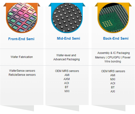
One of the hot topics in semiconductor engineering right now is 3D design. While this is being tackled in a few forms, the need to go 3D is simple – the reduction of distance and with that, resistance/temperature. This is one of the main factors driving the density (in terms of the number of connections in a given space) of devices and with that the challenges in inspection. Given that, high-resolution imaging is clearly required as well as multiple techniques and technologies. So is the need to implement these at different stages of the design and production process (Figure 3).
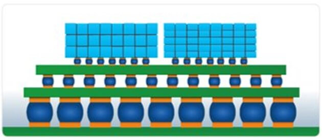
We have already established that this also makes sense in terms of the cost of failure by capturing the defects early before you have invested too much. It also follows that inspection at the early stages is also generally easier. For example, finding void defects in wafer bumps (Figure 4) before any other layers have been added, compared to a fully formed chiplet consisting of multiple devices, substrates, and interconnection layers (Figure 5).
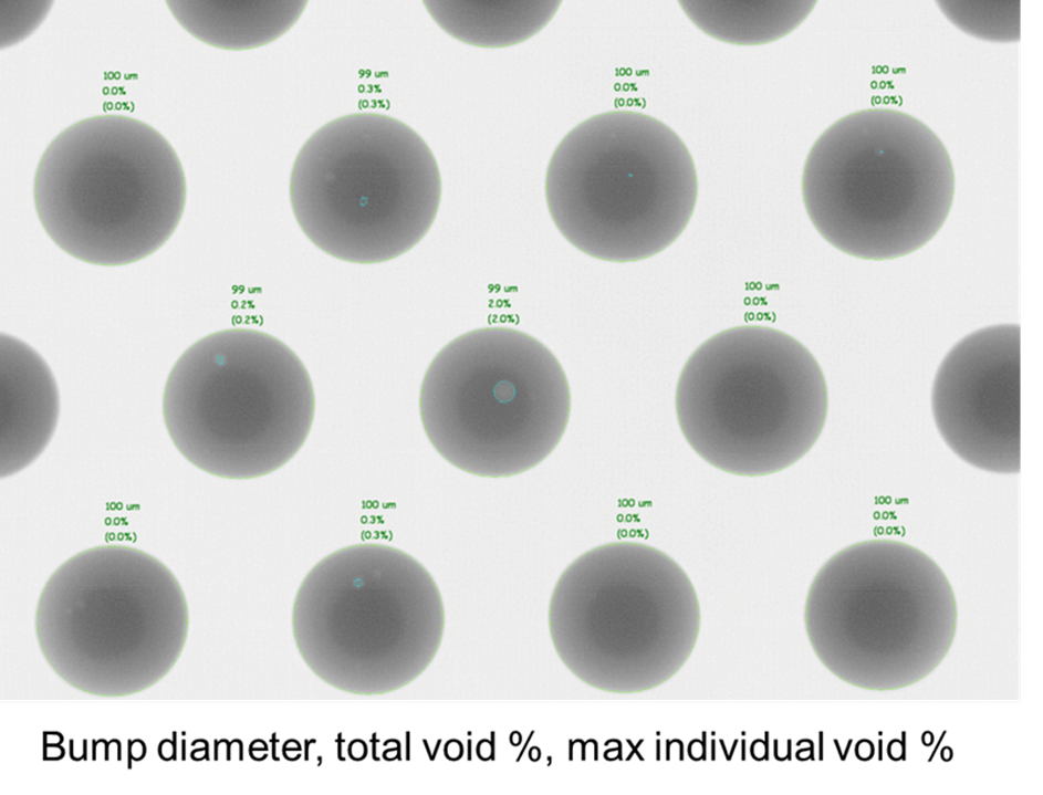
Figure 4. 100µm bump inspection.
This works out well. A simple inspection can be done with faster, more cost-effective 2D imaging, and then each of these elements is combined when proven good. At the same time, the quality of how these have been put together can then be inspected with the faster 3D techniques. When any of these devices are then found to have failed, more time can be justified to gain more detail and this insight can be fed back to improve process or design.
QUADRA 7 PRO – Brand New, Yet Proven
 During years of success with the main manual X-ray inspection system series called QUADRA, Nordson has been working in the background to introduce innovative, new core technologies with the Dual Mode X-ray tube and the Onyx X-ray flat panel detector, creating higher image quality across a wider range of applications.
The Dual Mode Quadra NT4® tube provides users with maximum flexibility. This innovative feature offers brightness and resolution modes, allowing operators to dynamically switch between them based on specific application requirements.
The newly-developed Revalution software is designed specifically for high-end semiconductor applications and provides an easy-to-use intuitive interface, optimized workflow, and expanded functionality, Revalution software empowers operators to efficiently analyze and interpret inspection data, enabling faster decision-making and improving overall productivity.
QUADRA PRO is taking the technology from the QUADRA SERIES and advancing it to an even greater level as the next generation of high-resolution X-ray inspection, focused on the challenges of the semiconductor industry.