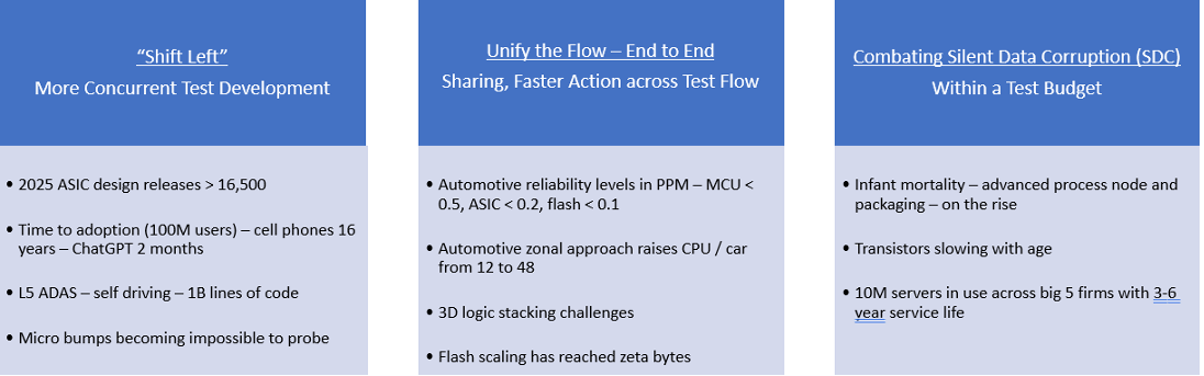
Is semiconductor device test non-value added? Certainly, some aspects are unchanging. Test is one of the three means to guarantee parts in addition to characterization and the design itself. Given the market backdrop – across automotive, computing, and advanced packaging – new test challenges and value adds have emerged. Three main themes are “shift left”, which is the need for more concurrent development with ever-increasing dependencies between design, packaging, test, and field operation; greater unification in development, production, and across the end-to-end test flow; and the continued war on silent data corruption (SDC) – balanced with test economics (Figure 1).
What is Shift Left?
The term “Shift Left” has been used increasingly within development to indicate tasks that were once performed sequentially but must now be done concurrently. This is usually due to tightening dependencies between tasks. Several types of “design for…” approaches are taking hold as tools within a broader design for test (DFT) umbrella: S (stress), R (reliability), I (inspection), and O (observability). Beyond test, some automotive firms are using S (security) and S (safety).
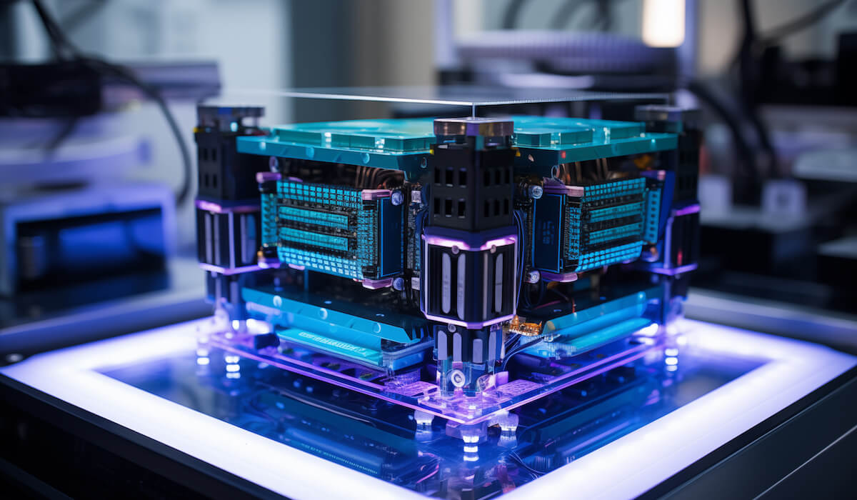
In simpler products wafer probe was an acceptable means for determining Known Good Die (KGD) as a gross screen before assembly. Now there is far too much value in an 8 FET SiC module [1] or 2.5/3D compute multichip modules such as system-in-package (SiP) and chiplets. The probe must produce as close to KGD as possible. With many forms of advanced packaging, all the interconnects must be checked regardless of accessibility – hence the term known good stack (KGS) and overall known good system (KGS).
The Universal Chiplet Interconnect Express (UCIe) specification [2], aimed at die-to-die, has been upgraded to 1.1 addressing more protocols and broader usage models. As 3D die stacking evolves from high-bandwidth memory (HBM) memory to logic, there are new challenges especially when using logic from various process nodes. One example is new physical stress mechanisms and a higher probability of interconnect failures.
The IEEE 1838 specification for die-to-die stacks is another example of a “shift left” in bringing design and test closer. KGx starts with the architecture and product planning, needs to be supported by the design, and is delivered by test and assembly operations.
More complex test flows and more expensive bill-of-material (BoMs) require greater unification across the end-to-end test flow for development and action in production.
Automated test equipment (ATE) and system-level test (SLT) linkage shows a huge increase in the need for SLT after ATE test. SLT can be as much as 50-100x less expensive than ATE, but it historically has been an “island” running very different and long (think 20 minutes) algorithms reflective of end customer use cases.
Intel notes that many of its customers run SLT for much longer periods than the company does. Many advances by Teradyne and Advantest facilitate more feed-forward and feedback of test patterns from the two environments to make initial test development results in improved reaction times to enhance upstream ATE test when new failure modes appear at SLT. Other examples include doing more analytics on the tester on the fly. The benefits of this include adaptive tests. For example, if a given batch of material (wafers, finished goods) is exhibiting certain parametric around process corners (fast/slow transistors, high/low power) then the test program can be adaptively and dynamically varied. ATE makers have placed more of these tools within the tester for real-time decision-making, as opposed to a central test floor computer.
At IEEE ITC in October 2023, Cariad (the electronics arm of Volkswagen) pointed out that testing for ADAS L4 and L5 environments generates a lot of data that, at present, is a missed opportunity for analysis/action. The unification of ATE tests would eliminate the overlap and duplication that come from how test was historically done, with batteries of tests from silos of R&D, quality assurance, security, and product/test/design organizations.

Can We Eliminate Silent Data Corruptions?
All these advances in testing and unification are nice – but why are very subtle, silent data corruptions (SDC) still happening in the field? Is the answer more testing? They are silent and even if the mechanism is discovered, then additional testing adds expense.
At IEEE ITC 2023, there was an excellent panel discussion on SDC about how to catch them in manufacturing, do advanced defect models, improve screening, and the benefits of telemetry. Overall, two main causes were highlighted: Good old-fashioned random points defects and more systemic parametric type failures within complex designs.
The point defects can be time zero test escapes or defects that just require a little bit of ‘activation’ time to emerge. Can more “intelligent” high voltage tests be invoked? The more sinister examples, although parametric in nature, involve very small delay effects and/or voltage droops under complex power schemes and situations. It begs the question – can more be done in design/validation to cover proper IC workloads? More specifically, if a part is said to be “pass” or “fail”, then the entire condition set needs to be understood ie: at what frequency at what voltage? A multi-layer approach is needed. Should quiescent current testing/fingerprinting be brought back? But after all these efforts – will we merely find the easy mechanisms and the hard ones will continue to elude us?
In summary, the industry drivers, such as automotive, compute, and advanced process/package nodes; combined with the never-ending quest to be smaller, better, faster, and cheaper – continue to result in new test challenges. More “shift left” is needed in test to speed up and improve the quality of development. Standards such as IEEE 1838 and UCIe 1.1 are steps in the right direction. Greater unification is happening across the test process flow, including linking SLT and ATE test more closely, and moving more ‘on the fly’ analytics to the tester for real-time reaction. Lastly, SDC is on the rise and is very hard to solve in a cost-effective manner.
[1] “SiC MOSFET Challenges, Demand and Industrialization of Test & Burn-in” – Mark Berry, 3D InCites, [2] “Update on UCIe” – Mark Berry, 3D InCites, October 2022November 2022
This article originally appeared in the 2024 3D InCites Yearbook.