
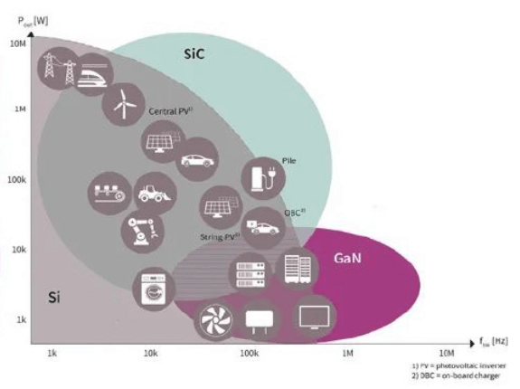
The coming-of-age and breakthroughs offered by silicon carbide (SiC) MOSFETs, as well as demand that is outstripping supply are rapidly driving improvements in processing, yield, and reliability learning cycles, and needs for greater industrialization of test & burn-in. SiC MOSFETs offer better overall performance, higher efficiencies, higher switching frequencies, and smaller footprints as compared to Si MOSFETs. They excel in areas of high temperature, high power, and higher switching speeds. Many applications reap huge benefits here – electric vehicles (including hybrids), wind turbines, railways, and data centers (Figure 1). Let’s take a deeper look at the demand and supply, the special material considerations, and the industrialization of test & burn-in needed to keep pace.
Demand & Supply
In 2021, according to Yole Développment, SiC device revenue was ~$1.75B and is expected to exceed $6B by 2027. SiC MOSFET in-vehicle EV demand was <150,000 wafers (200mm equivalents) but is estimated to exceed 4M by 2030. On the supply side – there’s little to no overlap to leverage silicon-based wafer fabs – hence a lot of new capacity is needed. IDMs are also moving towards vertical integration in terms of not only fabricating SiC MOSFETs but also to growing the actual boules of SiC wafers. Announcements in 2021 by Onsemi, ST Microelectronics, Wolfspeed, SK Siltron and Infineon about new fabs and expansions add up to ~$5B across next several years. ST also has a $800M agreement with Wolfspeed for wafer supply. Rohm and II-VI have also announced investments to increase substrate R&D and capacity. Even the EMS industry is engaging – with a $108M investment by Foxconn.
Technical Challenges
The overall state of SiC MOSFET yield, reliability, and costs are ~30 years behind Si. Yield loss is estimated to drive 30% of the product cost. Therefore, much innovation, Kaizen focus, and accelerated learning cycles are needed. Examples include:
- Growing the starting wafer – silicon melts at 2570°F versus 4946°F for SiC (proprietary furnaces)
- SiC crystalline growth takes 7 days versus 3.5 days for silicon
- Typically, an epitaxial layer of SiC is formed atop the SiC wafer – ~200 types of poly structures/defect points are possible
- 150mm SiC wafer runs ~$800 versus $265 for silicon
- High defect density and lower purity (as compared to Si)
- SiC transparency at visible optical wavelengths and high surface reflectivity impact inspection and metrology
- Gate oxide growth is not as easy or perfect as Si
- Slicing and grinding – SiC is the 2nd hardest material on earth (diamond is #1). It is very brittle and slicing/grinding can induce defects (much more so than in Si).
Test, Burn-in & Reliability
While basic tests and reliability stresses are similar across many types of MOSFETs and guidelines such as JEDEC JC-70.2 exist, many more test/reliability screens are required. There are some new or more serious issues around SiC: design can rely on electric fields 10X higher than silicon, asymmetrical gate voltage, threshold Vth drift, drafting, and bipolar degradation. Various instabilities must be checked, for example, voltage instability at 300°C in addition to 150-175°C standard tests. Voltage ranges started with 650V, moved to 1200V, then overstresses to 1700V, and new requirements for 2500V stresses and future paths go to 3300V. Care must be taken in the event of short-circuit events. Protection circuits are a must and are typically invoked before the start of the test and turned off immediately after; typically on the order of 100(s) of nanoseconds via ATE test systems (or FPGA(s)). Numerous ATE tester companies have entered the power module market – including Focused Test, Teradyne (Lemsys), Crea, Keysight, Chroma & Unites. There are also some new offerings in wafer-level burn-in (WLBI).
As with several other markets, known tested die (KTD) and now as close to known good die (KGD) and even known reliable die (KRD) is a must. This started with wafer level processing (WLP) – including fan-in wafer level chip scale packages (WLCSP) and fan-out wafer level packaging (FOWLP) – and gained relevance in early system-in-package (SiP), which are manifested today with advanced packaging. Early 2.5D for high-performance computing and today’s 2.5/3D/chiplets acting as alternatives to cost reduction deviations to Moore’s law, where sub 7nm SoC(s) are becoming too cost prohibitive. Power modules typically based on eight SiC MOSFETs run ~$80/module. To bring down a module with a poorly tested non-KGD, non-KRD single MOSFET is unacceptable. The cost/benefit tradeoff has shifted. Given these factors, there’s been an innovative upsurge around wafer level burn-in (WLBI) and higher concentration of wafer probe sort.
Advanced WLBI offerings from PentaMaster accommodate two wafers and x720 parallelism. AEHR also has a leapfrog solution with a proprietary wafer “clamshell” such that thin brittle SiC MOSFET wafers with specialized probe needles for the high-power aspects can be embedded in the shell and then moved to b) the FOX-NPTM high capacity WLBI tool capable of 18 wafers. Such WLBI systems for SiC MOSFET applications also have IR sensors for DUT monitoring, sealed chambers with capabilities for N2 gas, and special arc suppression gases. These higher-capacity tools require much less floor space and offer higher throughput than earlier burn-in tools.
Overall test and burn-in flows for SiC MOSFETs are running in the range of 2 to 4 days with 48-to-1000-hour burn-in. Further work is needed to reduce floor space and energy consumption (for example 20K watts per day are needed for burning in 100(s) of devices per load for a 1200 V / 80 mOhm FET at 20 A, 1000 V, 125C, 1000 hours).

Conclusion
SiC MOSFETs provide a leapfrog improvement in performance, higher efficiencies, higher switching frequencies, and smaller footprints. Tradeoffs include significantly different starting material processing, wafer fabrication steps, and equipment, as well as reliability screening, test, and burn-in. Overall SiC MOSFET maturity in cost and reliability is ~30 years behind Si MOSFETs, but opportunities exist – via novel testing, burn-in, and reliability test – that can speed up learning cycles accelerating improvements to the point of diminishing return (Kaizen).