November 2020 saw the 7th IEEE International Workshop on Testing 3D, Chiplet-Based, and Stacked ICs (which IFTLE has been calling the 3D Test Workshop), held in conjunction with the IEEE International Test Conference (ITC). It was spearheaded again by Erik Jan Marinisssen of IMEC and Yervant Zorian of Synopsys.
IMEC – Co-packaged Optics

The plenary lecture of the symposium was given by Joris Van Campenhout of IMEC. Campenhout relates that large installations such as hyper-scale cloud centers require long interconnect reach (500+ meters). Increasing compute demands in artificial intelligence (AI) and high-performance computing (HPC) are driving the need for faster and more scalable interconnects in the package/board and rack/cluster levels.
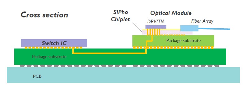
Scaling to 51.2 Tbps switch capacity and beyond is challenging using pluggable optics. Moving the optics closer to the switch IC can address power and bandwidth challenges. Many companies such as Microsoft and Facebook are developing so-called co-packaged optics (CPO).
CPO requires optical modules and silicon photonics chiplets with bandwidth beyond 3.2Tbps (Figure 1).
Silicon photonics seeks to leverage the existing CMOS infrastructure for photonic integration. In Figure 2 we see examples of the integration of passive and active optical functions in Si and Ge on a wafer.
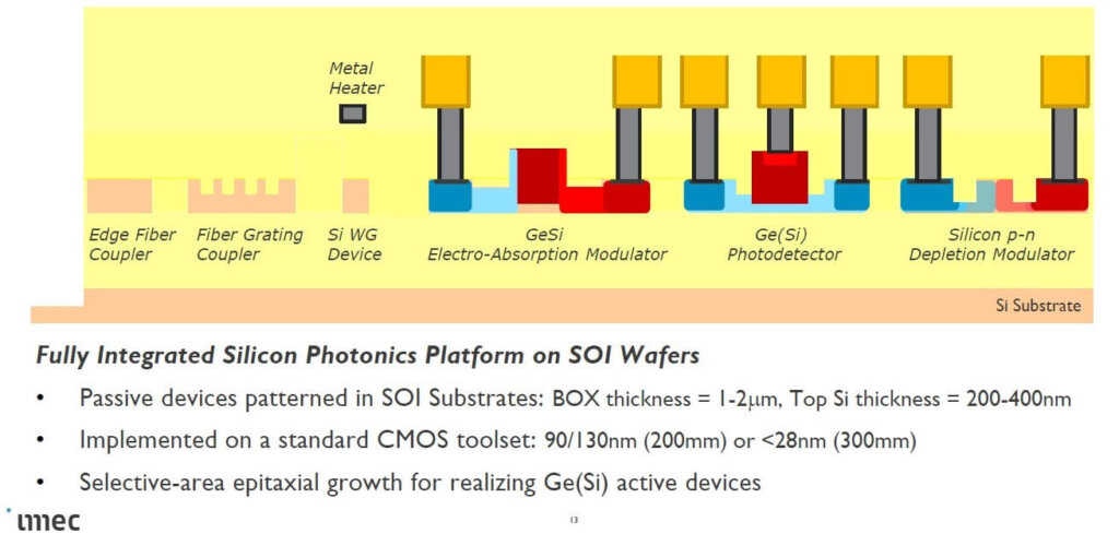
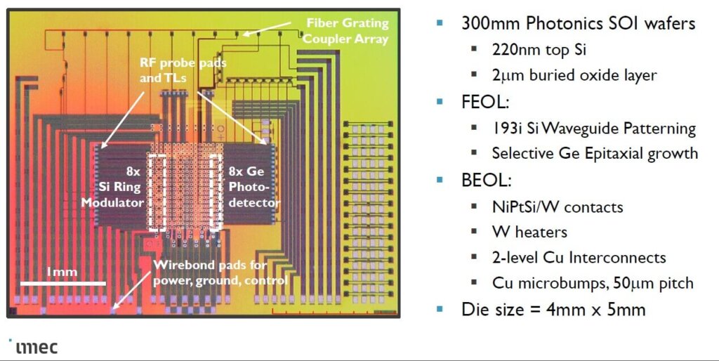
Figure 3 shows the IMEC silicon photonics test chip:
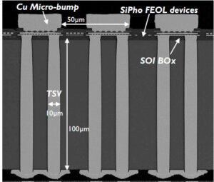
Silicon photonics transceivers are powered and controlled using through-silicon vias (TSVs) implemented in a silicon interposer shown in Figure 4. This results in bandwidth > 1Tbps/mm.
The remainder of the presentation discussed the protocols put in place for electro-optic testing these devices leveraging the test solutions for high bandwidth memory (HBM) and wide I/O interfaces.

Intel – Foveros Testing
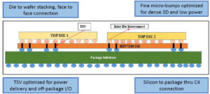
Lim and co-workers discussed the “Intel Foveros Technology: DFT and HVM Test Strategy”. “Foveros” is Intel’s 3D technology that allows logic chips to be stacked (Figure 5).
- Wafer-level testing is done thru the µBump, which has a smaller pitch vs. a regular C4 bump.
- Stringent selection in deciding which µBump signals needs to be probed
- Critical signals must have design-for-test (DFT) survivability and override options
- Ensure sufficient µbumps are probed to deliver sufficient power during various testing scenarios
TSV Testing:
- Mandatory parametric testing: Vcc-continuity/open/shorts testing/leakage
- A combination of HVM tests is needed to narrow down whether a defect is due to TSV or otherwise.
- Further failure analysis can then be done on the unit
- The key is to ensure that all TSVs are covered in testing!
3D Stack IC Test Access Mechanism:
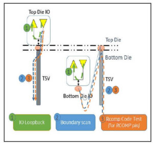
Test access ports for top die can be designed to be driven (Figure 6):
- i) Directly thru the TSV to the top die
- ii) Bottom die IO pins going thru the inter-die interconnect to the targeted top die
Considerations:
- Alternative test access path for top die
- Parallelism testing for top die and bottom die
- Singular reusable ATE test vector across different test access ports
- Flexibility to respond to the different market segments where primary test access mechanism might be no longer accessible (attaching DRAM, EMIB bridge, etc.)
For all the latest in Advanced Packaging stay linked to IFTLE……………………………………..