In 1965 Gordon Moore proclaimed that there would be a “’Day of Reckoning’ when it may prove to be more economical to build large systems out of smaller functions…”. The 2022 IEEE International Test Conference, held live and in-person for the first time since the pandemic, addressed the implications of this proclamation on semiconductor test protocols.
Plenary talks by Lawrence Berkeley National Labs1 and Google2 – set the stage for needed advances and approaches involving chiplets and hyper-scale data centers:
- 8% of the world’s power is used for data centers – projected to drive 40% by 2040 (untenable at current trajectory)
- There is still a 3-to-6 orders of magnitude shortfall in computing power needed for the full realization of virtual/augmented reality, artificial intelligence, machine learning, remote intelligence, and autonomous vehicles.
- “Post CMOS extreme heterogeneity” is needed – leveraging open domain-specific architecture (ODSA) and Universal Chiplet Interconnect Express™ (UCIe™)
- Key aspects of ODSA include open die-to-die (D2D) interfaces, reference designs, and workflow
- The semiconductor industry cannot continue to spin all chips from scratch; hence the need for a “chiplet and licensable IP ecosystem: IP is the commodity (not the chip)” and “what is the right partnership/economic model for the future of HPC”?
- Third-party assembly was also mentioned as part of this new economic model
- A chiplet marketplace to “integrate best-in-class chiplets from multiple vendors”
As SoC(s) begin to hit cost and complexity walls, there’s a huge push to advanced package, multi-chip approaches, including novel approaches using chiplets. Typical advanced 2.5/3D packaging has traditionally been a route taken by a singular processor IDM working with memory IDMs – the “disintegration” of SoC(s) into chiplets allows for other IDM’s offerings to be selected, fostering an open motherboard approach.
Sounds good, right? Well, how do different silicon providers agree on inter-chip communications that support system validation? In comes the “UCIe™, an open specification that defines the interconnect between chiplets within a package, enabling an open chiplet ecosystem and ubiquitous interconnect at the package level.” The presentations on UCIe™ can be summarized as current status, test challenges, and way forward.
Current Status
The UCIe™ specification has reached a revision 1.0 level and is backed by AMD, ARM, Google, Meta, Microsoft, Qualcomm, and Samsung. Other major backers with cited 2.5/3D packaging are Intel (EMIB), ASE-SPIL (FoCoS), and TSMC (CoWoS).
Chiplet approaches in processor systems result in caps on SerDes rates slowing the processor but allowing for more of them for bandwidth – claiming three order-of-magnitude improvements in bandwidth density.
UCIe™ revision 1.0 is well positioned for the next 5-6 years. Aspects such as phy layers, protocol specs and provisions for thousands of lanes are addressed – supporting up to 32GB/sec with < 2ns of physical transition delay.

Test Considerations
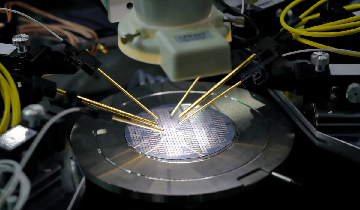
AMD presented comparisons of monolithic SoC processors versus chiplet-based systems, contending that traditional test approaches result in a 2x increase in the number of required scan modes and patterns plus a whopping 5x jump in test time.3 This is driven by several additional ‘in-situ’ test insertion points in the assembly flow. They referred to a “pre-bond” die test (chiplets and processor), a “mid-bond” point after stacking, and a “post bond” final test including “down” configurations consisting of passive dummies and partially working salvageable die. And lastly, AMD reported on a more generic test strategy using package broadcast, on-die scan comparators (ODSC), and “accelerated fly-overs” to leverage re-use, shorten test development times and reduce bring-up overhead.
Chiplets also pose test challenges in compliance, debugging, and observability. One step forward is the IEEE 1838 standard for test access architecture in stacked die systems. An interesting system test load board concept is to socket the given chiplet (device under test or DUT) onto a final product-like system board – with the actual silicon bridge, interposer or other interconnect method routed over to a reference, known good die – typically the processor.4
Way Forward
Other big picture paths for chiplets and UCIe™ :
- Data centers run at only 35% utilization with 65% “marooned” resources at any given time. UCIe™ can be extended beyond the package into system “re-timers” to access different parts of the system rack thereby raising utilization.
- Hints were also given that there may be ways to design chiplet-based systems to be able to ride through failures.
- Future applications could also be very effective in silicon photonics – enabling optical components to be co-packaged with SoC(s).
Summary
At current trajectories, today’s semiconductor systems won’t be tenable for power consumption and won’t meet computing requirements. Rises in 5nm and below design and mask set costs also pose huge economic barriers. Alternatives using chiplets present a more viable path. Initial UCIe™ rev 1.0 enables a foundation for the next 5 – 6 years.
References from ITC 2022
- “The Future of High-Performance Computing Beyond Moore’s Law” – John Shalf, Lawrence Berkeley National Labs
- “Make Computing Count: Some Grand Opportunities for Testing” – Parthasarathan Rangnanthan
- “Chiplet Level Test Parallelism for 3D Stacking Projects”, A. Margulis, et. al.
- “Road to Chiplets: UCIe™” – portion of a special session presented by D.D. Sharma of Intel