

At the Intel “architecture day” held Dec 12th in Santa Clara, Intel finally announced what some of us have been waiting for, literally for over a decade.
The Foveros Backstory
In late 2006, CEO Paul Otellini displayed a 300mm wafer of 80 core microprocessors (Figure 1) and announced that such technology would soon be in production. In 2007 Bryan Black (later of AMD), Morrow and other Intel researchers described their work in both memory-to-logic and logic-to-logic stacking with TSVs.[1]
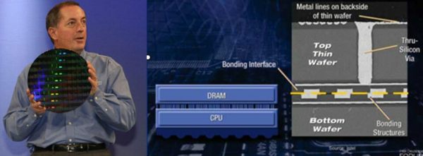
During the 4th 3D-ASIP conference, December 2007, Intel’s Jerry Bautista commented that there were no remaining technical issues and that Intel was ready to commercialize their 3D integration technology “…as soon as the product groups decided which product to insert the technology into.” He felt the most likely candidate would be high-performance computing (HPC). He showed us a picture of a 300mm wafer that reportedly contained DRAM bonded to CPU with Cu-Cu thermos-compression bonding at a 10µm pitch (as shown below)
That certainly was a strong enough trigger for many of us to declare “3DIC has arrived!”
While it has been reported that Intel is using stacked memory in their “Knights Landing” Zenon Phi HPC CPU module, which started shipping in 2016, [see IFTLE 198 “IFTLE 198 Intel & Micron HMC 3D Stacked memory…”] the use of 3D stacking involving dis-integration of the CPU has been rumored but never announced.
Still in the Game
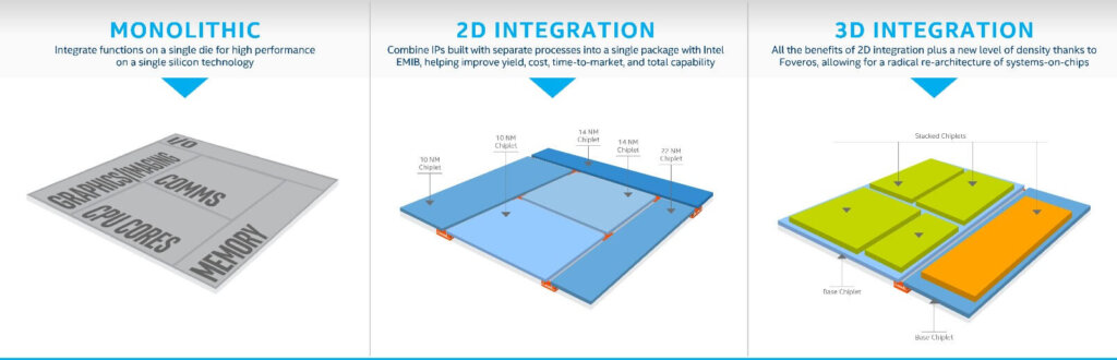
In recent months Intel’s reputation has taken several hits after TSMC and Samsung have announced scaling moves from 14nm to 10nm to 7nm while Intel appeared stuck at 14nm by publically postponing their move to 10nm several times. This week’s Intel announcement certainly is a statement that they are still in the game and intend on using a combination of chiplet technology architecture and 3DIC stacking packaging technologies to gain performance advantages on the competition (Figure 2).
Intel has named their stacking technology “Foveros,” Googling this Greek word turned up the following:
Not sure IFTLE would have picked a term that could mean “fearful” or “horrifying”, but it is now a word that will become part of our Advanced Packaging lexicon…so learn it!
What Foveros Does
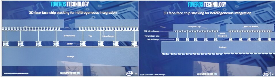
Foveros allows for 3D face-to-face (F2F) stacking for integration of many different types of devices on an active TSV interposer, which then sits in the package (Figure 2. The Intel Foveros technology is not simply an interposer like those being used in AMD’s Fiji or NVIDIA’s GPUs. Low-power components such as I/O and power delivery will be put into a base die, with high-performance logic stacked on top.
Intel indicates that it will separate the various processor components into smaller chiplets, each of which can be manufactured using an optimum (performance/cost) production node (Just like IFTLE and others have been preaching for more than a decade). Thus, Intel could deliver “10nm CPUs”, which could have 14nm and 22nm chiplet modules within them (Figure 3). So, memory, graphics, power regulation, and artificial intelligence (AI) function could all constitute separate chiplets, some of which could be stacked through TSV. For further info on chiplet technology see IFTLE 396 “DARPA Envisions CHIPS as a new approach to Chip Design and Manufacture”
While memory stacking using TSV technology has been commercialized by Samsung and Hynix for several years now, Intel will be the first to bring 3-DIC stacking to logic-logic integration and functions such as CPU, graphics, and AI processors.
With Foveros, the most important element is not necessarily the speed of each individual chiplet on the package, but instead the speed of all elements working together in each specific application case. Intel claims Foveros can be produced in volume. They claim it is not just for specialized or customized processors, but also for mainstream CPUs.

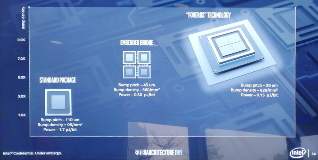
With Intel EMIB technology, components can be tightly packaged together side by side. Foveros appears to enable greater density and a reduced footprint.
Bump pitch has been reduced to 36µm as shown in Figure 5, meaning more I/O per unit area, i.e. higher density.
While Intel did not discuss their solutions for power delivery and testing, they indicated that rigorous testing, a new power delivery process, and a new insulation material to dissipate the heat has helped the company avoid the typical 3DIC stacking problems.
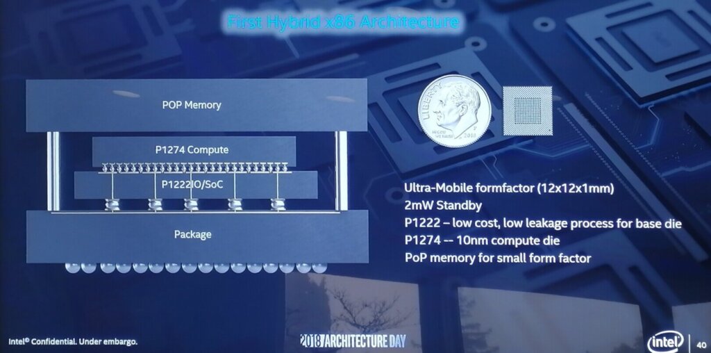
Intel says that Foveros products will be shipping in the second half of 2019 The first products will combine 10nm compute logic stacked on top of a base die using the company’s 22FFL (FinFET Low power) process, topped off with package-on-package memory FIgure 5). This chip will be aimed at ultra-mobile systems with the processor measuring 12×12×1mm and having a standby power of 2mW.
AMD has also recently announced that its next-generation Zen 2 processors will be separating its CPU logic from I/O. The CPU logic will be on 7nm chiplets and everything else will be on a separate 14nm I/O die and will double core counts.
For all the latest in Advanced Packaging stay linked to IFTLE……………………..
References:
[1] P. Garrou “3D Commercial Activity”, chapter 15 in Handbook of 3D Integration, Garrou, Bower, Ramm Eds., Wiley VCH (2008)


