

In September of 2018, I spoke with KLA’s Stephen Hiebert and Pieter Vandewalle about the changing advanced packaging landscape, and the need for better process control that inspired the company’s foray into the advanced packaging space. With the introduction of its IC packaging portfolio that comprised the Kronos™ 1080 and the ICOS™ F160, KLA was able to apply its front-end process control and inspection know-how to address the needs for improved reliability and yields of high-value advanced packages, particularly high-density fan-out (HDFO).
A lot has happened in those two years. As an industry, we’ve experienced tremendous growth in these high-value advanced packages, including HDFO, 2.5D, 3D ICs, driven by the need for artificial intelligence (AI) and machine learning (ML) technology, as well as high-performance computing applications such as data centers and 5G networks and base stations. And then there’s the automotive market, with its focus on electric vehicles (EVs) and advanced driver assist systems (ADAS), that call for a variety of packages of different types, all of which must be reliable and robust enough to withstand extreme environments. Lastly, and perhaps most importantly, is the rapid acceleration of chiplet technologies, with all the major players introducing variations on the theme.
What’s Different about High-Value Advanced Packages
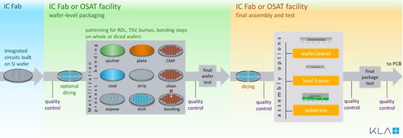
All of these high-value advanced packages are upping the ante for process control and inspection solutions that identify and sort defects to separate the known good die (KGD) from the bad, inspect advanced packages from all angles, and sort and bin final packages (Figure 1). KLA heard the call, and recently introduced its next generation of advanced packaging systems, that have all been enhanced to serve these needs. I recently chatted with Hiebert and Vandewalle to learn more.
Vandewalle described a convergence across all manufacturing segments – front-end, back-end packaging, and surface mount technology (SMT). “There is so much change – from materials used, interconnects and feature sizes, and accommodating custom product shapes – for example, hearables,” he explained. “It’s a very dynamic environment and it creates a lot of opportunities.”
Although multi-die packaging began years ago with the introduction of package-on-package (PoP), early fan-out (FO) architectures, and 2.5D integration, it’s just now hitting the big time. For example, Vandewalle noted that RF packages for 5G often have upwards of 30 dies mounted everywhere – top, sides, and bottom. This is driving new and more complex inspection needs.
Vandewalle explained that when it comes to process control and inspection system enhancements, it all boils down to two aspects: more intelligent sorting for finished package inspection and minimizing yield loss for finished and non-finished components. This is what drove the enhancements for the suite of WLP and finished inspection products, he explained.
“The concept of known good die (KGD) is becoming more critical, especially for high-value advanced packages. One failing die can cause a several-hundred-dollar package to fail and this is unacceptable,” he said, adding that as packages become more complex, so do the upstream inspection needs, including outgoing quality control, in-line process control, and engineering-phase yield improvements.
Wafer-level Packaging Defect Inspection
According to Hiebert, the first-generation wafer level inspection tool, Kronos 1080, was the outcome of customer collaborations to combine KLA’s front-end expertise with wafer inspection, combining them to address emerging challenges. As high-value advanced packages continue to evolve, the next-generation version, Kronos 1190, has evolved right alongside, addressing additional challenges such as new materials, more complex process steps, shorter product life cycles, increased customer quality requirements, and new failure mechanisms.
“Both high-density fan-out and 3D stacking with and without die-to-wafer hybrid bonding are very challenging front-end type processes used to enable heterogeneous integration and higher density interconnection between die at the wafer level.” Said Hiebert. These more complicated processes require advanced process control to make the final products more robust and bring them to market. He said the tool is designed to help during the early stages of development during defect discovery and engineering analysis.

So, what has been enhanced in the Kronos 1190? With a focus on sensitive defect inspection, the tool is equipped with high-resolution optics to capture finer WLP features during in-line process control. More complexity means more process steps, all operating on high-value die from front-end fabs. “This is challenging to yield in the first place. If there are any WLP process excursions, they need to be detected as fast as possible, so they can be corrected quickly,” explained Hiebert. This also makes it possible to continually make incremental improvements in baseline yield.
The system implements deep learning and artificial intelligence (AI) to improve sensitivity, productivity, and particularly classification accuracy for identifying and separating critical and non-critical defects. This provides customers with more accurate defect information so they can take the correct action, whether that is yield improvements or screening and binning. The system also has the capability to use design input to lock in the most important inspection areas on the wafer, improving its inspection precision and fine-tuning results.
Sorting Die to Assemble High-Value Packages
After wafer inspection, die sorting for stage one quality control is critical. It comes with its own set of challenges, such as separating out the good parts from the bad parts in a high-volume manufacturing environment after dies have been tested and diced. Defects that happen during dicing, such as low-k sidewall cracks and laser grooves, cannot be detected with traditional visual inspection.
According to Vandewalle, the ICOS F160XP system combines optical and true IR side inspection in a single module to provide efficient inspection flow with high-sensitivity to the hairline cracks that can occur in high-value fan-in packaged, memory chips, and bare die to avoid integrating bad die in the final package.
Final Sort for High-Value Packages
The second quality control gate happens after the final package test, during the final sort tray-to-tray or tray-to-tape. High-value advanced packages, which come in more shapes and sizes than ever, have made this a particularly challenging endeavor. They have more complex features with smaller defects, stricter tolerances for modular assembly, and generally higher quality requirements. According to Vandewalle, the next generation of the ICOS T3/T7 Series provides sensitivity to defects and accurate 3D metrology, allowing package manufacturers to accurately sort components and improve their yield at a low cost of ownership.
Some packages, such as those used for 5G connectivity, have different requirements based on the end-use application. Take, for example, 5G devices that are used in both mobile phone applications and ADAS systems for vehicle-to-vehicle communications. While the devices are the same, the automotive reliability requirements are stricter. There is an advantage to being able to sort these components into different grades for use in different applications requiring different levels of reliability.
The ICOS T3/T7 series does just that, notes Vandewalle. It uses AI for smarter binning of defect types, providing accurate feedback on package quality to sort parts without operator review “This makes it possible to dial-up or down what defects you want to capture,” he said.
Further details about KLA’s enhanced suite of tools for process control, inspection, and sorting of high-value packages can be found here.


