
We have known for some time that with scaling coming to an end the industry would need to find another way to continue moving forward. One of the options is known as SoC disintegration, which is when a system-on-chip (SoC) is disintegrated into its functional parts and then connect these “chiplets” back together. Chiplets are not simply small chips. They cannot be used by themselves but are specifically intended to be interconnected together to build complete functionality. Thus, it is better to think of chiplets as a silicon IP (intellectual property) subsystem, designed to integrate with other chiplets through advanced package interconnect (usually micro bumps) and standardized interfaces. Building chips from pre-verified chiplets is beginning to gain traction as a way of cutting costs and reducing time to market for heterogeneous designs.
My first concepts of SoC disintegration and chiplet technology came in the early 2000s when the industry began seriously looking at 3DIC technology and what advantages 3D would have over standard system-on-chip SoC technology. From the 5000-foot perspective, it was clear that what we were really heading towards was the separation of functions, as shown in Figure 1 from a side I first used in 2005. At that time, I was espousing in my presentations and advanced packaging blog IFTLE that, in the future, functions would be manufactured as separate chiplets, using the best technology and node, and recombined on high-density substrates to form a multichip module with near SoC performance.
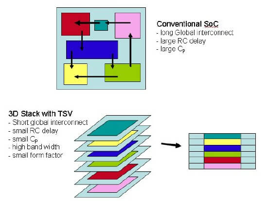
Figure 1: An early diagram of how SoC could be partitioned into separate functions and re-integrated vertically into a 3D stacked IC.
These thoughts were modified as it became clear that heterogeneous 3D stacking would be a complex undertaking (chiplet sizes, matching I/O, standard interfaces, etc.) and would instead be proceeded by what is now called 2.5D integration, where the functions could be manufactured separately, at optimum technology and optimum node, and combined on a high-density interposer.
The first commercial entity I saw express similar ideas was AMD’s Bryan Black at Georgia Tech’s Global Interposer Conference in 2011. Brian noted that the Southbridge at 22nm would probably be the last AMD chip impacted by scaling and that in the future “…separately fabricated functionalities would be combined vertically or horizontally on an interposer to form the final circuit function” (Figure 2).

Xilinx had already announced the production of their 28nm Virtex 7 FPGA in 2010, but that’s not what we are talking about now. Xilinx broke a large chip into 4 equal pieces and recombined it on an interposer to achieve higher yield and near-equal performance. Here we are separating by function, optimizing process yield, and recombining. The question was, would that ever be an economic solution, and could the current infrastructure ever support such a contrarian concept?
Marvell’s MoChi
In 2015, Marvell announced its modular chip architecture (“MoChi”), which they described as a virtual SoC. Rather than integrating as many functions as possible into an IC (the SoC concept), the MoChi approach focused on splitting an SoC into chiplets of specific functions, that could be connected with each other without compromising the overall system performance. Although this was reportedly being commercialized in internal Marvell products, the technology did not gain traction or much attention outside Marvell.1
DARPA’s CHIPS
In 2015, Dan Green and DARPA had similar yet slightly different thoughts from the DoD perspective.2 The department of defense (DoD) was having trouble gaining access to the latest chip nodes and packaging technology. By definition, they would always have a high number of part types but low volume runs for each part. This was not exactly the type of orders Intel, TSMC, Samsung, ASE or Amkor were/are looking for. But, what if each piece of IP in an SoC could be fabricated into small chiplets, tested and standardized so they could “talk” to other chiplets, and be available as standard chiplet parts at a given node?
Thus, the basic idea is that you have a library of chiplets. By assembling the required chiplets (functions) and connecting them using a standardized die-to-die interconnect scheme, you could develop new systems required by the DoD. In theory, the chiplet approach could be a fast and less expensive way to procure such devices. It’s certainly been proven for SoC products that reuse of IPs have enabled people to create advanced designs in a much faster timeframe.
In theory, you could have a large catalog of chiplets from various IC vendors. Then, you can mix-and-match them to build a system. Chiplets could be made at different process nodes and re-used in different designs (Figure 3).

The DoD DARPA program, Common Heterogeneous Integration and IP Reuse Strategies (CHIPS), began in 2017 involving various types of contractors/sub-contractors including Intel, Northrop, Micross, Ferric, Jariet, Micron, EDA suppliers Synopsys and Cadence, and several universities including Michigan, UCLA, and Georgia Tech.
With chiplets, the designer could focus on designing at a higher level by integrating known and trusted chiplet functionalities, but there appeared to be two main obstacles that needed solutions before chiplet technology could be looked at as mainstream:
- Chiplets from different sources MUST have standardized interfaces/communication protocols.
- Currently, at least three options are under serious evaluation. Intel has developed AIB and MDIO, TSMC has developed Lipincon, and the Open Domain-Specific Architecture (ODSA) has created the CDX (Chiplet Design Exchange) to standardize design.
Known-good Die (KGD)
Using chiplets takes us back to the KGD conundrum from the early MCM days in the 1990s. The purchaser of a chiplet, requires virtually 100% yield, i.e. a fully tested and qualified KGD. Also ensuring that the connections between the chiplets on the substrate/board are properly tested, is essential.
Several companies are working on a variety of interposers and bridge technology, which is less expensive than an interposer. Intel already has its embedded multi-die interconnect bridge (EMIB), and Samsung has announced a redistribution layer (RDL) bridge for wafer-level packaging.
Commercialization
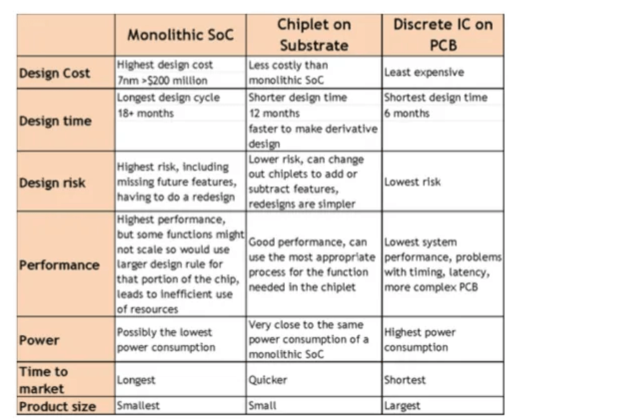
Both technically and financially, the industry’s traditional method of building increasingly larger chips has become less and less appealing. So, major semiconductor companies are designing products that break the larger designs into smaller pieces (“chiplets”) and combine them. A comparison of monolithic vs. chiplet solutions are shown in Figure 4.
In the last 24 months or so we have seen AMD, Intel, TSMC, and Samsung adopt chiplet solutions.
AMD’s Approach to SoC Disintegration
In 2017 AMD used chiplets in their “Zen 2” architecture to develop the Epyc server processor “Naples”. AMD engineers estimated an SoC design would have more than doubled the manufacturing cost and significantly increased the development time. AMD is now deploying its “Zen 2” chiplet technology in Ryzen 3rd Generation consumer CPUs (Ryzen 3000s) and AMD’s next-generation enterprise EPYC processor, known as Rome.3
The IO die for the EPYC Rome processors uses Global Foundries’ 14nm process, however, the consumer processor IO dies (which are smaller and contain fewer features) are built on the Global Foundries 12nm process. The EPYC Rome processors, built on these Zen 2 chiplets, will have up to eight of them, enabling a platform that can support up to 64 cores. As with the consumer processors, no chiplet can communicate directly with each other — each chiplet will only connect directly to the central IO die. That IO die houses links for eight memory channels and up to 128 lanes of PCIe 4.0 connectivity (Figure 5).
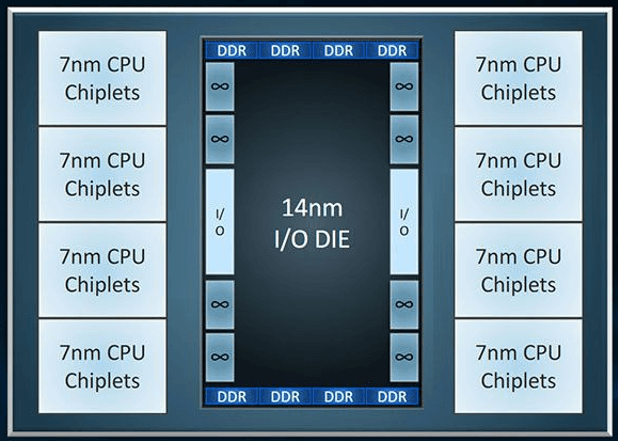
The IO die controls off-chip communications, housing PCIe lanes for the processor, memory channels, and links to other chiplets or other CPUs.
The consumer processors, Ryzen 3rd Gen or Ryzen 3000, will be offered with up to two chiplets for sixteen cores.
AMD is using “Infinity Fabric” (IF), (their interconnect protocol, NOT something Thor and Iron Man acquired from Thanos) to connect chiplets and the DDR DRAM interfaces. The IF protocol can run on any hardware in which it is implemented. IF can run through PCB traces, an interposer or EMIB, as long as both connected dies support it.
Separating CPU chiplets from the I/O die has its advantages because it enables AMD to make the CPU chiplets smaller thus using less 7NM technology theoretically making the module less expensive to manufacture.
Intel’s Approach to SoC Disintegration
Intel’s EMIB technology basically uses small silicon interposers to connect (i.e. bridge) two chiplets through microbump (~ 55um pitch) interconnect.4
The EMIB is embedded into a high-density PCB packaging substrate. Intel claims this results in lower cost since the whole substrate does not need to be high cost 2.5D silicon, but some outside Intel are not convinced that these specialty PCB substrates with embedded silicon are as simple to make or cheap to buy as Intel infers. Intel reports that they currently have two solutions based on EMIB.
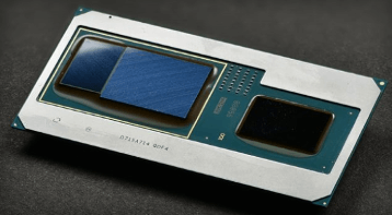
Kaby Lake-G integrates an AMD Radeon graphics processor unit (GPU) with a high bandwidth memory (HBM) memory stack and an Intel computer processor unit (CPU) chip (Figure 6). Kaby Lake uses an HBM interface inside the package to integrate the GPU and HBM and PCI Express, a standard circuit-board-level interface, to integrate the GPU and the CPU.
The Stratix 10 FPGA has an Intel FPGA and six chiplets (Four high-speed transceiver chiplets, and two HBM chiplets) and they are all assembled in a package (Figure 7). This example integrates six different technology nodes from three different foundries.
Stratix 10 uses the Intel-developed Advanced Interface Bus (AIB), which was created for this product as the high-bandwidth, logic-to-logic interconnect inside the package. The AIB interface can be used both with Intel’s EMIB interconnect solution and other solutions such as silicon interposers. AIB is currently the standard interconnect of choice in DARPA’s CHIPS program.
Chiplet Standardization
To get widespread adoption of chiplet technology we must have standardization of the I/O interfaces. i.e. a chiplet made by company A must be able to talk to a chiplet made by company B. The DARPA CHIPS program has focused on the Intel AIB protocol. More recently, TSMC, who is fabricating chiplets for AMD announced its “Lipincon” protocol. 5
In September, the Chiplet Design Exchange (CDX) [zGlue, Ayar Labs, Avera Semi, ASE, Cadence, Netronome, and Sarcina] announced, as part of the Open Compute Project (OCP), a subproject to standardize design automation for the impending chiplet marketplace. The group is tasked with standardizing machine-readable chiplet models to enable chiplet catalogs and provide reference flows for the development of chiplet-based modules.
CDX plans to create a proof-of-concept based on PCIe while developing its PHY, protocol, and other specs. The group also aims to define a business flow for chiplets and define a test certification for known good chiplets. EE Times reports that the group “appears to have rejected Intel’s AIB protocol as being too limited in data rates and pinouts.” 6
In conclusion, the disintegration of traditional SoC technology appears to be underway!
This article first appeared in the 3D InCites Yearbook. Download your copy here.
References
- W. G. Wong, Q&A: A Deeper Look at Marvell’s MoChi Technology, Electronic Design, June 6, 2016. https://www.electronicdesign.com/technologies/digital-ics/article/21801569/qa-a-deeper-look-at-marvells-mochi-technology
- P. Garrou, IFTLE 396: DARPA Envisions CHIPS as New Approach to Chip Design and Manufacturing, 3D InCites, October 17, 2018, https://www.3dincites.com/2018/10/iftle-396-darpa-envisions-chips-as-new-approach-to-chip-design-and-manufacturing/
- I. Cutress, AMD Zen 2 Microarchitecture Analysis: Ryzen 3000 and EPYC Rome, AnandTech, June 10, 2019: https://www.anandtech.com/show/14525/amd-zen-2-microarchitecture-analysis-ryzen-3000-and-epyc-rome
- S.K. Moore, Intel’s View of the Chiplet Revolution IEEE Spectrum, April, 2019 https://spectrum.ieee.org/tech-talk/semiconductors/processors/intels-view-of-the-chiplet-revolution#qaTopicOne
- P. Garrou, IFTLE 427: TSMC’s Next-Gen 3D Technology – N3XT, 3D InCites October 4, 2019 https://www.3dincites.com/2019/10/iftle-127-tsmcs-next-gen-3d-technology-n3xt/
- R. Merrit, Chiplet Effort Plays First Proposals EETimes, March 29, 2019 https://www.eetimes.com/chiplet-effort-plays-first-proposals/


Comments are closed.