

This year’s keynote talks at the 2016 IMAPS Device Packaging Conference (DPC 2016) provided some new insight into a number of interesting areas of importance to the advanced packaging community. I already addressed Bill Chen’s talk, which focused on system-in-package (SiP) and introduced a 3D Fan-out SiP approach. Here, I’ll focus on the key take-aways from the other three keynote talks that focused on Intel’s embedded multi-die interconnect bridge (EMIB) technology, imec’s 3D technology landscape, and Broadpak’s in-depth look at security issues with 2.5D and 3D technologies.
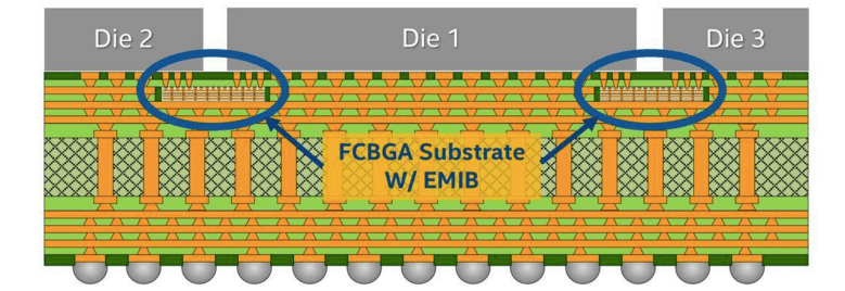
Ravi Mahajan, Intel, kicked off this year’s even with a discussion about EMIB, which some classify as a fan-out wafer level technology (FOWLP), but seems to me to be an embedded die/interposer technology. Mahajan classified it as an on-silicon wiring approach that does not use through silicon vias (TSVs), but still provides improved bandwidth and density. He said traditional wire length for on-substrate wiring is up to 70mm. EMIB can achieve a similar length to Si interposer (~0.5mm to 10mm) through the use of embedded, thin silicon “bridges” that take the place of a full-size Si interposer. These are strategically located only in the few areas that high-density, multi-chip package connections are needed, rather than as a full-size Si interposer (Figure 1).
Because EMIB doesn’t require TSVs, a number of process steps are eliminated including TSV formation and fill, and TSV reveal and backside processes. Instead, the Si die are integrated into the package substrate, followed by typical 2.5D assembly. As such, in terms of overall cost, Mahajan says EMIB is better choice than Si interposer integration. Attendees posed questions about the reliability the CTE mismatch. Mahajan said he’s concerned about everything until it works; so far, EMIB works, and any CTE issues are manageable.

Mahajan also talked about the increasing demand for on-package CPU/memory bandwidth and capacity. Although Intel has integrated a version of the hybrid memory cube (HMC) into its Knight’s Landing Processor (he called it MC-DRAM), Mahajan said high bandwidth memory (HBM) has higher bandwidth than MC-CDRAM and is emerging as the memory-of-choice. While EMIB has not yet been used to package HBM, Mahajan says it is compatible with the technology, as it offers localized high-density interconnects to enable high bandwidth links. Currently, EMIB has been used to package Altera’s Stratix 10 FPGA.
imec’s 3D Technology Landscape
Gilbert Beyer, imec, followed Mahajan, and brought us up-to-date on some of the latest 3D integration technology advancements that are underway at imec.
Beyer began his talk by explaining why imec refers to the 3D technology landscape versus the 3D technology roadmap. “’Roadmap’ is very linear. For 3D, that’s clearly not the case. There are lots of options that coexist at the same time,” he explained.
imec has defined three main classes of 3D integration: 3D stacked IC (3D SIC), 3D system on chip (3D SOC) and 3D IC. Wiring and partitioning levels that require different process schemes, and achieve progressively smaller contact pitches differentiate them. 3D SiC requires global-level wiring, is partitioned at the die level and achieves pitches down to 5µm. 3D SOC has a range of wiring options including semi-global, intermediate, and local, and achieves pitches from 5µm down to 100nm at the local level. 3D SiC partitioning is achieved using die-to-wafer or die-to-interposer stacking. Depending on the partitioning level and pitch requirements, 3D SOC is achieved through wafer-to-wafer bonding in parallel, or through sequential processes using active layer bonding or deposition processes. 3D IC takes places at the transistor level, and uses active layer bonding or deposition processes in sequential processes.
Beyer focused the remainder of his talk on the latest technology advances to scale wafer bumping, and in wafer-to-wafer bonding. “We are confident that we can create smaller diameter TSVs,” he noted. “The concern is the die-to-die interconnect pitch. The state of µbump pitch is a significant mismatch with TSV interconnect density capability.”
While bumps have scaled successfully to 10µm, beyond that the challenges increase. Mechanical stability, alignment of the bonder, and bump slide-off are all issues. imec has been investigating a technique to embed µbumps in polymer. Cu damascene processes are used to realize the bumps, explained Beyer. While some questioned the cost of such a process, he said it doesn’t have to be more expensive because you perform passivation processes either way.
Beyer also talked about hybrid and dielectric bonding for wafer-to-wafer bonding schemes. While dielectric bonding doesn’t create an electrical connection between the two wafers, it is possible to introduce TSV via last after the wafers are bonded, achieving smaller diameter vias than with traditional TSV via last approaches.
Beyer’s concluding message is that 3D interconnect enables chip-to-chip connections for 3D SiC and 3D SOC. Scaling of key components of these technologies will enable higher interconnect densities; in particular TSVs, µbumps, and hybrid bonding. He also stressed that this is not an either/or situation. 3D interconnect technologies will co-exist, possibly even within the same system.

Securing SiPs
So as to not present a commercial for his company, Broadpak, Farhang Yazdani, focused his 3D keynote on security concerns we are facing due to the IoT rather than solutions; but rest assured, his company has solutions to the hardware security issues, in particular.
Any connected thing can be tampered with to carry out an action, noted Yazdani. For example, he cited the now-famous hacked Jeep, and also noted that an implanted medical device (IMD) can be un-secure, and can lead to catastrophic results if hacked.
Software assumes that the “core root of trust” is secure, but Yazdani says the reality is that it is not. Hardware security is a grave concern. “You might have developed a great product that is a great engineering achievement, but it’s a goldmine for intruders, and open to sniffing, spying, and tampering,” he said. An un-secure IoT SiP may not give you the right data; it may send data to other sources; it may perform tasks other than what it was intended for; or it may be activated or deactivated by adversaries. All of this can happen a number of ways: cyber attack through the network, through IP, through tampering with the chip, or a side-channel attack.
Hardware attacks, which are Broadpak’s focus for its advanced packaging solutions, can happen a number of ways. Cloning involves copying existing products and inserting malicious logic, idle channels, power and timing variations, test ports, tampering, and reverse-engineering so that you can probe the design and build your own. Overbuilding beyond the original PO is another way to do this. Design defects can be use to break into the device. Tampering allows for unauthorized access to the hardware through ‘back doors’.
Yazdani detailed the numerous points in the supply chain that pose potential security risks: On the design front, specs, tools and library models; IP development; and design-for-test (DFT) are all sensitive areas. Even more risky is during the manufacturing, and assembly processes; particularly front-end mask processes, wafer probe, packaging and test. The possibilities are somewhat mind-boggling.
For example, deleting or adding traces, or changing metallization can be done to introduce a Trojan. Additionally, changing the doping area changes the device functionality. Changing 128 bits to a random number of bits can reduce the security of a product.
Yazdani concluded his presentation by saying that Broadpak’s focus is on security, and that the company provides secure, tamper-resistant, anti-cloning technologies.
While this does nothing for the millions of un-secure devices already out in the world, at least going forward with new products, we know that solutions are available. ~ FvT


