
As we all know, finding thermal management solutions is becoming an increasingly critical but also an ever more challenging issue for the semiconductor industry as the power density increases while the semiconductor packaging structure becomes more complex. Thermal dissipation is often a great concern as the power density of the semiconductor devices increases and the junction temperature rises, which can adversely affect the performance and reliability of the semiconductor device.
Effective tools and capabilities are needed to develop thermal management solutions to ensure that the performance of the semiconductor devices is not adversely affected by poor thermal performance. Both computer simulation and physical thermal testing play important roles.
Computer simulation can evaluate different design options, perform sensitivity analysis, and help the designer select the best solution among those multiple options – without having to build actual prototypes. This is very useful in the early development of a new product (such as a semiconductor device), and it greatly helps accelerate product development. The advantages of computer simulation are obvious and for this reason, computer simulation has been broadly utilized as a tool in product development for semiconductor devices over the years.
However, this is not to say that computer simulation can completely replace physical measurements and testing because computer simulation typically suffers from several very significant limitations. To begin with, computer modeling always needs to make a certain number of assumptions – regarding the boundary conditions, the ambient conditions, materials properties, etc. Often, simplifications must be made for a complex structure – especially as the semiconductor packaging structure becomes more complex. Heterogeneous integration makes these issues even more challenging as a large variety of materials, interconnects and interfaces are often involved in a single package – all very important elements in the local eco-system for the thermal performance of the semiconductor package.
Further, computer modeling often deals with a static problem while the real problem is always a dynamic one. For example, materials properties, such as the thermal interface materials (TIMs) can vary and can change over time under environmental conditions. Pump-out can happen under thermal and mechanical loading. It is often difficult for computer simulation to precisely consider all these variations. There is also non-uniformity in the various elements of the structure – in the chip, in the heat sink, in the TIM, etc., and it is difficult to precisely account for all these real-life non-uniform conditions in the computer simulation.
Very importantly, the interface between the various elements and materials (such as the die, the TIM, and the heat sink) in the package structure plays significant roles in heat dissipation but is quite difficult to precisely characterize in terms of the thermal resistance, and computer modeling often needs to make simplifications in these complex packaging structures. Real-life functional semiconductor devices are also very dynamic in terms of their thermal behaviors, especially when there are interactive effects, for example between materials properties and the device temperature which the properties of the material directly affect; These dynamic and interactive phenomena can be difficult for computer modeling to capture precisely.
In real life, failure modes and performance degradation mechanisms are often complex, and computer modeling typically is focused on a few known failure modes. Unforeseen failure modes for a particular semiconductor package can sometimes pose significant risks. As such, physical testing is always needed for validation.
Of course, thermal measurements and testing have their own challenges – especially when the testing needs to be performed before the actual semiconductor device has been developed and manufactured – which may take several years. The industry practice has been to develop thermal management solutions – which require thermal measurements and testing – as the chip is developed. Thermal test chips (TTC) and thermal test vehicles (TTV) play important roles in this concurrent environment (Figures 1 & 2).
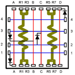
The TTCs must be able to closely approximate the power input and power density distribution of the chip (typically non-uniform), and simultaneously accurately sense the temperature distribution (using integrated sensors) over the entire die (with resolution down to 1mmx1mm), in real-time.
Interestingly, as the TTCs are as small as 1mm2, they can be very useful for simulating the thermal performance of chiplets for advanced semiconductor devices.

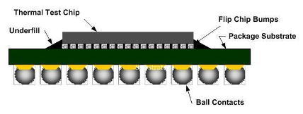
The TTVs, consisting of a packaged TTC(s), must be configured to represent the intended packaging structure, and constructed and manufactured using the actual TIMs, heat sinks, and other real components that can affect the heat dissipation and thermal performance of the entire system. Industry standards such as JEDEC JESD51-series standards must be strictly observed for comparison of alternative thermal management solutions. TTVs can also be constructed for a specific application with the real package structure – which is often different (and more complex) from the package structures defined in the standard. As such, TTV’s can have many specific varieties (Figure 3).
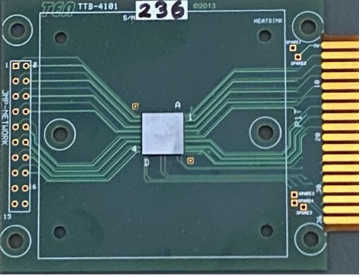
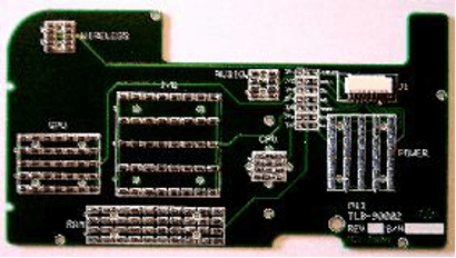
Thermal load boards (TLB) are system-level thermal management design tools for the concurrent design of the mechanical, electrical, and thermal aspects of electronic systems (Figure 5). The TLB is typically custom designed to provide a close physical simulation of the actual thermal load conditions using resistive and TTC Heat Source Simulators (HSS).
These tools are very useful for characterizing the thermal performance of semiconductor devices and packages. Using the TTCs and TTVs, and by performing thermal measurements and testing in real-life environments (such as the power input, the ambient conditions, airflow, etc.), the spatial and temporal temperature distribution (including hot spots) over the chip can be characterized, the thermal performance of the entire package can be assessed, the various package design, TIMs, heat sinks, etc., can be evaluated, and the computer modeling can be calibrated and validated.
Overall, our goal in product development for semiconductor devices is to have “optimal design” – not over-design (which affects cost, size, weight, and TTM), or under-design (which affects reliability and product performance). The only way to get there is through the effective use of computer simulation (“digital twin”) in tandem with thermal measurements and testing – using “physical simulation” (“physical twin”).
For further information, please contact Dr. Dongkai Shangguan.