

The CHIPS Act, which is finally gaining some momentum in Congress, is looking at how to improve the United States’ competitiveness as well as supply chain in the semiconductor development and manufacturing space. From the conversations being floated, there appear to be two major concerns: 1) has the U.S. lost its advanced technology edge? And 2) how does the U.S. improve its supply chain to avoid shortages? Figure 1 presents data that suggests that the U.S. still has a strong technology edge, or at least a design edge, but has shipped most of the manufacturing overseas for economic reasons. Qualcomm, Nvidia, AMD, and Intel all have chips manufactured and packaged in the Asia Pacific region.

Some off-hand hand comments during SEMI’s TechTalk on Heterogenous Integration at SEMICON West, were that it didn’t make sense to bring trailing-edge technology back to the US, but it was more important to bring back the leading edge, and advanced packaging. One can argue the lack of impact that will have on securing the supply chain. However, it’s entirely possible that Intel’s proposed factories in Ohio will be more foundry-related and dedicated to supplying trailing-edge foundry services to automotive and industrial companies looking for an onshore supply of chips. This is especially true as electric vehicles (EVs) become more popular, a steady supply of chips will be needed to keep the automotive factories functional.
IEDM Demonstrates Technology Centers
However, the question, “Has the U.S. lost its technology edge?” had me looking at the recent IEDM conference and where 3D technology activity is happening. From my perspective, the IEDM gives a good snapshot of where technology development is taking place. In some cases, the technology will be released in a year or two, and in others the introduction, if it ever happens, is still five or more years away. At one time, the IEDM conference was “THE” conference to introduce new logic transistor or DRAM technology. This has changed a little bit, as Intel does not appear to be as active as they used to be due to concerns of giving away too much information about its technology advances.
As chips and transistors move forward to future technology nodes, the technology is converging in two directions. 1) Transistors are moving from finFETs to nanowires and nanoribbons to more monolithic structures where the transistors are stacked on top of each other rather than side to side, in the what is being called fork sheet and CFET structures. The second is where the industry is using heterogenous integration to either stack or in some cases build 3D structures to develop systems capable of performing modern compute more efficiently with hopefully means reduced power consumption. Each of these technologies are critical to improve chip performance and potentially reduce the power chips consume. The IEDM had five sessions covering each of these technologies. The first of these sessions was session three, and all of the papers were invited. The result of this section was an interesting cross section of 3D technologies. The papers that were presented included (note: Some of the titles have been shortened):
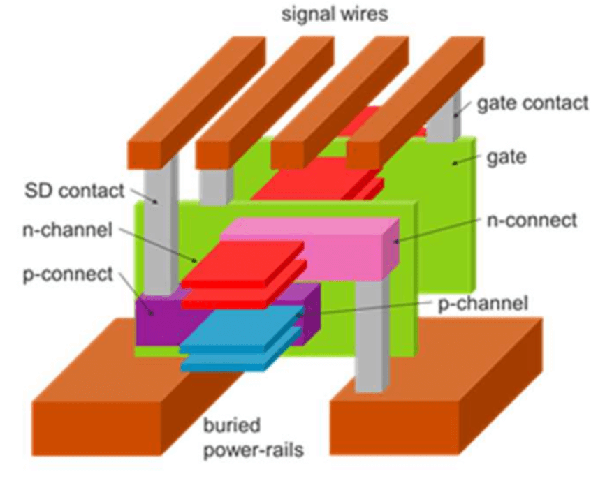
- TEL Technology Center, Albany Nano-tech, CFET Design Options
- CEA LETI, Sequential Processing for a Smart Imager
- Hitachi High Tech, IMEC, Inspection and Metrology Challenges for 3nm
- Synopsys, Heterogenous Integration Enabled by State-of-the-Art 3DIC Design and Modeling
- North Carolina State University, Design for 3D Stacked Circuits.
- IMEC, 3D SoC integration, beyond 2.5D chiplets
- TSMC, Foundry Perspectives on 2.5D/3D Integration and Roadmap
While papers from Intel and Samsung were missing from this session, from my perspective this gives a pretty good cross section of what is taking place in R&D across the industry. IMEC and CEA-LETI have been two of the leading research consortia in the 3D space; LETI for monolithic and packaging technology, and IMEC for next-generation transistors and 3D packaging research. Most of the leading chip companies like TSMC, Intel, Samsung and others participate in non-competitive research that takes place at these facilities.
University research does not often make it into the Day 1 morning session, so it was good to see North Carolina State University discussing some of the design issues facing 3D heterogenous integration. The paper from Synopsys, which had worldwide participation, also touched on the challenges of design, some of which were, heat, and the need for additional design tools to help make integration and design easier. The inclusion of NCSU and Synopsys, also helps to illustrate the path from fundamental research at a university, to applied research at a key supplier in the industry, which is needed to implement the tools to make the chip manufacturers successful.
The TEL Technology Center at Albany Nanotech continues to perform leading-edge research as diagramed in Figure 2, and is a key component of both IBM and Samsung transistor development.

The final two papers, by IMEC and TSMC, on 3D packaging, pointed out the advantages of moving to 3D packaging, and that the success of shrinking the bump pitch and interconnect will play a significant role in reducing the size of the final product, as well as the power the system consumes. Power reduction is becoming a more important issue in high-performance compute and will play a critical role in lowing the power in cloud computing facilities.
It’s an Integrated World
In reviewing the other advanced logic sessions that were showcased at IEDM, the authors were from around the world and in some instances, papers had authors that had collaborated from multiple universities, in different parts of the world.
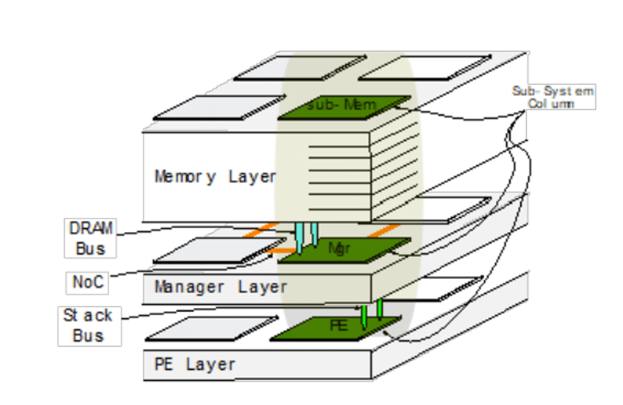
A good example of how 3D integration is generating collaboration across industry and universities is paper 25.4 from the memory-centric computing and 3D integration session. Figure 4 shows the authors’ thoughts on what is needed for future generations of compute using 3D integration to better mimic human thought and to develop new systems for artificial intelligence (AI). Contributors on this paper were from Stanford, MIT and Facebook, with additional funding from DARPA.
From looking at the logic papers that were presented at IEDM this year, it appears from a technology perspective, Figure 1 is not too far off. There is a great deal of technology and design that is generated in the US, a significant amount at universities, and supported by both US based companies and the US government. There is also a great deal of technology that is developed pre-competitively in Europe at IMEC and CEA-LETI, which then finds its way to manufacturing centers worldwide.
The microelectronics industry is truly a worldwide industry where technology can be developed in a university nearly anywhere in the world, made ready for manufacturing in Europe, designed in the United States, and then manufactured in Asia. While, bringing the manufacturing back to the United States is an interesting idea, what’s to keep it from moving overseas again when the economics become prohibitive to producing chips in the United States the next time? With any luck, over the next 6 months the CHIPS Act will pass. And hopefully, cities and regions in the United States will help to create the tax incentives that the foreign chip companies receive, to help keep US chip companies healthy and manufacturing in the US.


