
Latest Posts

Koh Young Webinar to Show How Data Transparency Strengthens SMT Production Resilience
Koh Young, the industry leader in True3D™ measurement-based inspection solutions, invites electronics manufacturing professionals to register for its upcoming webinar,...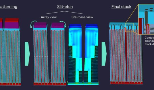
Mechanical Stress in Semiconductor Development
3D NAND subarray structures tilt during slit processing, demonstrating stress evolution, including deformation.
Digital and Physical: Thermal Twins for Developing Thermal Management Solutions
As we all know, finding thermal management solutions is becoming an increasingly critical but also an ever more challenging issue...
IFTLE 529: More Hybrid Bonding from ECTC 2022
Continuing our look at key Hybrid Bonding (HB) papers at the recent ECTC 2022 in San Diego, CA. Applied Materials...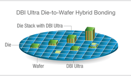
Xperi and Micron Enter Into License Agreement for Hybrid Bonding
Xperi’s IP Licensing Business Deepens its Presence in Memory Market SAN JOSE, Calif.–(BUSINESS WIRE)–Adeia, the newly launched brand for the...How MTP Technology Improves 3D Heterogeneous Integration
High-performance computing, communications, mobile, automotive, industrial, medical, and defense systems increasingly require 3D heterogeneous integration of many diverse components to...
3D Technology Development is a World-Wide Activity
The CHIPS Act, which is finally gaining some momentum in Congress, is looking at how to improve the United States’...
NHanced Semiconductors Launches High-Tech Nexus in Indiana
Will leverage next generation technologies, spur workforce development, seed small businesses NHanced Semiconductors announces a new office in the Westgate...
Cadence Integrity 3D-IC Platform Supports TSMC 3DFabric™ Technologies for Advanced Multi-Chiplet Designs
Cadence Design Systems, Inc. (Nasdaq: CDNS) today announced that it is working with TSMC to accelerate 3D-IC multi-chiplet design innovation....

IFTLE 500: We’ve Come a Long Way, Baby!
IFTLE (Insights From the Leading Edge), believe it or not, has reached #500! I hope this message reaches all of...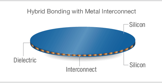
Xperi Licenses Hybrid Bonding Technology to Yangtze Memory Technologies Co., Ltd. (YMTC)
Direct Bond Interconnect (DBI®) hybrid bonding portfolio licensed to YMTC for its 3D NAND memory products SAN JOSE, Calif. –Xperi...
The 3D Era is Upon Us
Building integrated circuits (ICs) in the third dimension has been taking place since trench capacitors were introduced for DRAM in...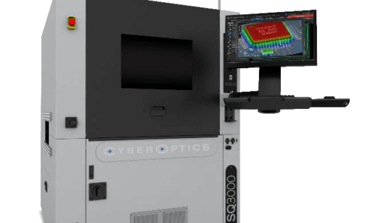
CyberOptics Highlights the New SQ3000™+ Inspection and Metrology System at NEPCON Asia
Minneapolis, Minnesota — September 16, 2021 — CyberOptics® Corporation (NASDAQ: CYBE), a leading global developer and manufacturer of high-precision 3D...
CyberOptics to Showcase High-Precision Inspection and Metrology Solutions at the SEMI Connecting Heterogeneous Systems Summit
Minneapolis, Minnesota — August 4, 2021 — CyberOptics® Corporation (NASDAQ: CYBE), a leading global developer and manufacturer of high-precision 3D...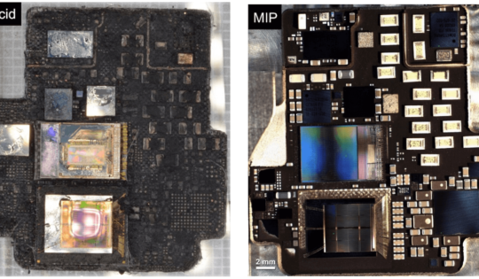
Artifact-free Decapsulation of 2.5D and 3D Advanced Packages
As semiconductor devices are subject to increasingly higher quality and reliability standards, extensive measures must be taken to ensure these...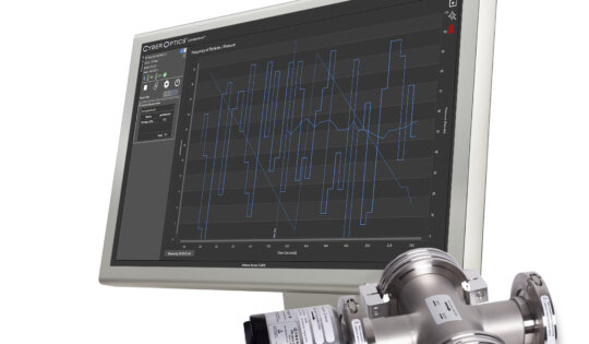
CyberOptics to Share Technical Presentation About Best-in-Class Airborne Particle Sensing Processes at PhotoMask Japan
Minneapolis, Minnesota — March 31, 2021 — CyberOptics® Corporation (NASDAQ: CYBE), a leading global developer and manufacturer of high-precision 3D...
3D: The El Dorado of Heterogeneous Integration
From the cloud to edge computing, the quest for ever-greater power efficiency remains researchers’ top priority. From high-end niche to...ASM Pacific Technology and EV Group Join Forces to Enable Industry’s First Ultra Precision Die-to-Wafer Hybrid Bonding Solutions for 3D-IC Heterogeneous Integration
Joint Development Program will offer highly configurable, ultra-precision end-to-end hybrid bonding solutions to suit various applications, with optimal line balancing...