
About X-Celeprint
About X-Celeprint, Ltd.
X-Celeprint licenses Micro Transfer Printing (MTP) technology, which consists of more than 300 worldwide patents and 189 pending applications, to support semiconductor manufacturers in adopting MTP. X-Celeprint is co-located with Micross, which has a Trusted/ITAR-compliant 200mm wafer fab with extensive heterogeneous capabilities, in Research Triangle Park, North Carolina, and Tyndall National Institute in Cork, Ireland. Both facilities have MTP technology in their R&D advanced packaging lines for supporting customers with rapid prototyping. X-Celeprint has research partnerships with academic centers, including the University of Illinois Urbana Champaign and the University of Ghent / imec.
Equipment maker ASM AMICRA supplies precision placement systems to implement X-Celeprint’s MTP technology, and X-FAB, the leading foundry for analog/mixed-signal and specialty semiconductor solutions, has licensed X-Celeprint’s MTP technology to support volume heterogeneous integration.
X-Celeprint Micro-Transfer Printing Technology
High-performance computing, communications, mobile, automotive, industrial, medical, and defense systems increasingly require 3D heterogeneous integration of many diverse components to improve their performance and functionality. These diverse components include high electron mobility transistors (HEMTs), heterojunction bipolar transistors (HBTs), power transistors, gate drivers, photonics, sensors, hardware assurance devices, capacitors, inductors, filters, and antennas manufactured using many different process nodes and technologies, including SOI, GaAs, GaN, InP, and SiGe.
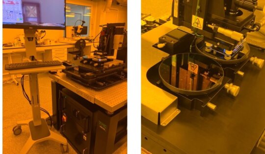
X-Celeprint’s micro-transfer printing (MTP) technology employs a massively parallel pick-and-place process to stack large arrays of ultra-thin (1-20 micron) diverse components, called x-chips, from one or more separately manufactured wafers on a variety of destination substrates to improve heterogeneous integration to create a 3D IC with the following improvements in:
- Performance – by re-partitioning, disaggregating, and re-integrating by stacking separately manufactured components
- Power – by reducing parasitics and resulting power losses by using ultra short interconnects
- Area – by using the z-dimension for integration rather than growing x- and y-dimensions and producing ultra-thin 3D ICs for embedding in substrates and organic interposers
- Cost – by separately manufacturing each component using the optimal material and technology node, reducing die size, increasing utilization of expensive semiconductor wafers, using low-cost, massively parallel manufacturing processes and relaxing manufacturing thermal constraints
- Time-to-market – by combining x-chips produced in different fabs and re-using them in multiple designs by stacking them in different configurations to manufacture many different 3D ICs
- Security – by integrating multiple hardware authentication and sensor x-chips
Authors
 Bob Conner
 X-Celeprint News
How MTP Technology Improves 3D Heterogeneous Integration
High-performance computing, communications, mobile, automotive, industrial, medical, and defense systems increasingly require 3D heterogeneous integration of many diverse components to...X-Celeprint Authors Articles
Workforce Development Considerations in the Megachips Era
Sep 13, 2022
A recent Wall Street Journal article, The Microchip Era Is...