High-performance computing, communications, mobile, automotive, industrial, medical, and defense systems increasingly require 3D heterogeneous integration of many diverse components to improve their performance and functionality. These diverse components include high electron mobility transistors (HEMTs), heterojunction bipolar transistors (HBTs), power transistors, gate drivers, photonics, sensors, hardware assurance devices, capacitors, inductors, filters, and antennas manufactured using many different process nodes and technologies, including SOI, GaAs, GaN, InP, and SiGe.
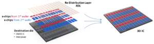
X-Celeprint’s micro-transfer printing (MTP) technology employs a massively parallel pick-and-place process to stack large arrays of ultra-thin (1-20 micron) diverse components, called x-chips, from one or more separately manufactured wafers on a variety of destination substrates to improve heterogeneous integration to create a 3D IC with the following improvements in:
- Performance – by re-partitioning, disaggregating, and re-integrating by stacking separately manufactured components
- Power – by reducing parasitics and resulting power losses by using ultra short interconnects
- Area – by using the z-dimension for integration rather than growing x- and y-dimensions and producing ultra-thin 3D ICs for embedding in substrates and organic interposers
- Cost – by separately manufacturing each component using the optimal material and technology node, reducing die size, increasing utilization of expensive semiconductor wafers, using low-cost, massively parallel manufacturing processes and relaxing manufacturing thermal constraints
- Time-to-market – by combining x-chips produced in different fabs and re-using them in multiple designs by stacking them in different configurations to manufacture many different 3D ICs
- Security – by integrating multiple hardware authentication and sensor x-chips
X-Celeprint’s MTP technology supplements other conventional and advanced packaging technologies, providing 3D IC manufacturers with a unique “tool-in-the-toolbox” optimized for heterogeneous integration of large arrays of ultra-thin, diverse components. An MTP-based 3D IC (Figure 1) is manufactured using the following steps: 1) Source wafer fabrication; 2) Destination wafer or substrate fabrication; 3) MTP stamp fabrication; 4) MTP pick-and-place; and 5) Thin film interconnects.
1) Source Wafer
Tightly packed x-chips are fabricated on source wafers made using the optimal process node and technology (such as SOI, GaN, GaAs, InP and SiGe) for each component. A sacrificial layer is formed underneath the x-chips using different techniques depending upon the source wafer technology, such as:
- For SOI x-chips on silicon wafers with <100> or <111> crystal plane orientation, a standard TMAH or KOH etch removes the silicon under the x-chips with the oxide beneath the x-chips serving as a barrier against etch of x-chips above.
- For compound semiconductors grown on silicon wafers with <100> or <111> crystal plane orientation, a TMAH etch removes the silicon under the x-chips while not removing the compound semiconductor x-chips.
- For compound semiconductors grown on native substrates, various lattice matched sacrificial layers can be used to undercut the x-chips.
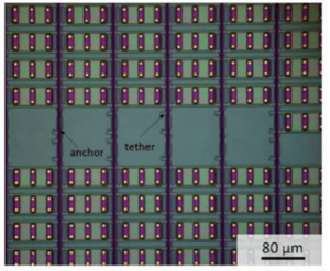
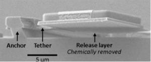
A tether/anchor system (Figures 2 and 3) holds the x-chips aloft after the source wafer is anisotropically etched to remove the sacrificial layer everywhere but underneath the anchor.
after partial x-chip pick-up
2) Destination Substrate
There are many options for the destination substrate, including silicon wafers with integrated CMOS ICs, silicon, glass, or ceramic interposer wafers, and large-area glass, ceramic, or plastic panels. The substrate’s surface may be planar or non-planar and be smooth or rough.
3) MTP Stamp Fabrication
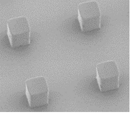
A low-cost, re-usable mold is used to make the MTP stamp (Figure 4) which consists of an array of soft posts composed of a compliant elastomer material, polydimethylsiloxane (PDMS), on a stiff glass substrate. The stamp is stiff in the x-y dimensions, providing high placement accuracy, and compliant in the z-dimension, accommodating non-planar and rough destination substrates. The post array on the stamp (Figure 5) is customized to match the desired destination substrate locations for massively parallel, selective pick-and-place of thousands of x-chips.
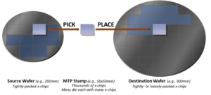
The stamp’s posts adhere to the x-chips via van der Waals force. The stamp’s viscoelastic behavior uses fast separation speed during pick-up to break the tethers and remove the x-chips, and slow separation speed to place the x-chips on the destination substrate. Using a “step and repeat” process, the entire destination substrate is populated with x-chips. The stamp can pick-and-place x-chips from smaller to larger wafers (Figure 6) with high wafer utilization, as the stamp readily handles x-chips at the wafer’s edge.

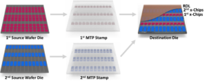
The x-chips may be transferred from multiple source wafers to different locations within the same die on the destination wafer to combine components made using multiple process technologies (Figure 7). By adjusting the pattern and spacing of the small posts on the transfer stamp, the x-chips may be tightly-packed on the source wafer, reducing cost via high wafer utilization, and either tightly- or loosely-packed on the destination wafer.
4) MTP Pick-and-Place
ASM AMICRA has been perfecting their ultra-high precision technology for almost 20 years, and supplies the following three systems to implement X-Celeprint’s MTP technology:
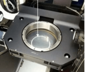
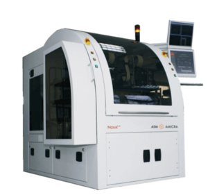
- The Nova+ MTP system (Figure 8) serves markets requiring high throughput. The fully automatic ISO class 4 clean room system employs a 50x50mm MTP stamp for massively parallel pick-and-place of x-chips from source wafers, which can be up to 300mm, to destination substrates, which can be up to 300mm wafers or 450x450mm panels. Placement accuracy is plus-or-minus 1.5-microns with a 40 second cycle time.
- The NANO MTP system serves markets, such as photonics, requiring more precise placement accuracy (plus-or-minus 0.5-micron).
- The AFC+ MTP system serves R&D and low volume manufacturing markets.
5) Thin Film Interconnects
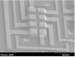
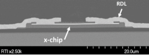
Since the x-chips are ultra-thin (1-20 micron), thin film interconnects may be readily used to connect the x-chips and destination die, resulting in very short path lengths, since both are active side up. Figures 9 and 10 show the top and cross section views of x-chips interconnected with a copper redistribution layer (RDL). The RDL provides a low electrical and thermal resistance path and enables use of multiple conventional and advanced packaging options.
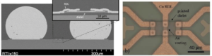
Figures 11 – 16 show a wide variety of prototypes manufactured using MTP:
|
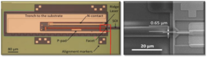
| 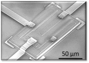 Figure 13: Integration of GaN HEMTs onto Silicon CMOS by Micro Transfer Printing Figure 13: Integration of GaN HEMTs onto Silicon CMOS by Micro Transfer Printing |
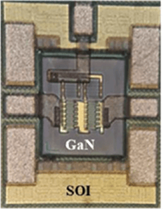
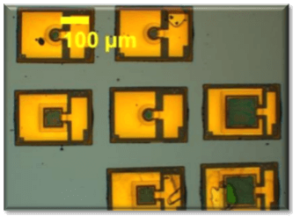 Figure 14:
 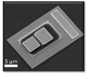 Figure 15: