 Riding the 3D/Heterogeneous Integration Wave
 Riding the 3D/Heterogeneous Integration Wave
For decades, the ability to achieve the necessary power, performance, area, and cost (PPAC) in semiconductor manufacturing had been largely driven by 2D design rule shrinks enabled through advances in lithography. In recent years, however, the rising costs and complexity associated with 2D shrinks have made it increasingly difficult to continue PPAC scaling on lithography advances alone. Indeed, many industry observers have noted this as a sign that Moore’s Law – the prediction that the number of transistors on an integrated circuit would double every other year – is either slowing down or is well and truly dead.
3D/Heterogeneous Integration in the Spotlight
The reality is more nuanced. While it is true that the constant pace of rising transistor counts on monolithic 2D semiconductors has slowed down, the industry has continued to successfully scale the PPAC metric by turning to 3D vertical stacking and heterogeneous integration – the manufacturing, assembly, and packaging of multiple different components and dies into a single device or package.
3D/heterogeneous integration enables high-bandwidth interconnects in advanced packaging to achieve overall system performance gains. As a result, they have become a crucial driver for AI, autonomous driving, and other high-performance computing applications. This is not to say that 2D transistor scaling via lithography is not important. Rather, 3D/heterogeneous integration is stepping into the spotlight and sharing the stage with lithographic scaling as equal partners in driving performance improvements on new semiconductor device generations.
Riding the Wave
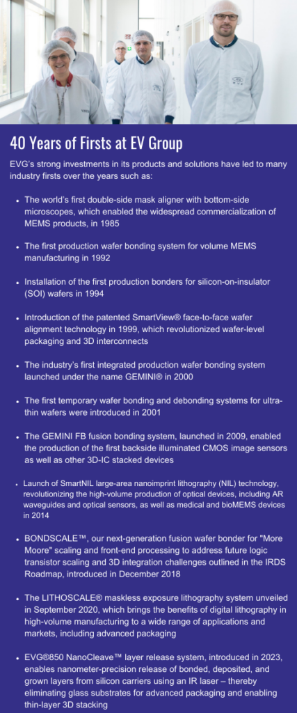
Since EV Group’s founding more than 40 years ago, our vision has been steadfast in “being the first in exploring new techniques and serving next-generation applications of micro- and nanofabrication technologies”. Our founders DI Erich and Aya Maria Thallner recognized from the beginning that semiconductor innovation requires a holistic approach – from the integration of new materials and material combinations to the integration of different layers, components, and device types. As a result, EVG has maintained a strong level of investment in our products and infrastructure over the years to pioneer advances in heterogeneous integration and wafer-level packaging. This has led to many industry firsts in wafer bonding, lithography, and metrology technology.
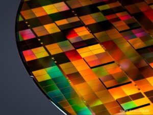
It’s no surprise that the increasing importance of 3D/heterogeneous integration in driving semiconductor innovation has coincided with an extended period of particularly strong growth at EVG. While demand has been on the rise across all of our major product areas, it has been particularly strong for our hybrid bonding solutions. The adoption of newer packaging technologies — from 2.5D to 3D system-in-chip (SiC) to 3D system-on-chip (SoC) — with tighter and tighter pitch requirements to support higher bandwidth needs are in turn fueling the need for new and different hybrid bonding techniques (Figure 1).
In addition to our strong R&D investments annually to develop new and innovative wafer bonding and other 3D/heterogeneous integration process solutions, EVG has significantly grown its headcount, process development, and production infrastructure to support our customers’ rapid growth and help them accelerate the deployment of their new products.
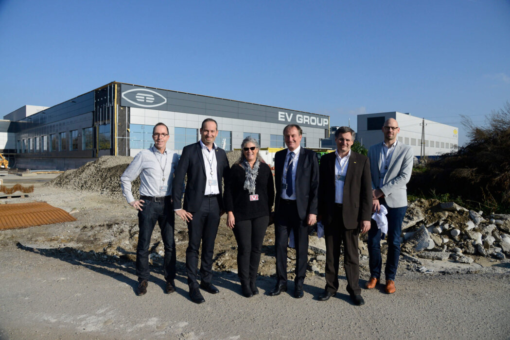
From our first manufacturing and assembly buildings at our headquarters, EVG has achieved consistent solid growth, with a surge in growth over the past few years. In 2018, EVG broke ground on our new Manufacturing III building near the River Inn, which doubled the floor space for the final assembly of EVG systems. We had the distinct pleasure of inviting the Queen of 3D herself, Françoise von Trapp, out to survey the site of our new building (Figure 2), which was completed in 2019. From there, our growth has continued at a strong pace to meet the ever-growing demands of our global customer base for our industry-leading process solutions.
EVG opened our Manufacturing IV facility at the end of last year and we have just completed and opened our Manufacturing V facility, which serves as the manufacturing department for EVG product components. The ultra-modern facility is fully air-conditioned with humidification and dehumidification systems and features 200 m2 of window area offering lots of natural sunlight in addition to LED lighting throughout. In addition, it is ergonomically designed so that no objects need to be lifted by hand. Hydraulic lift platforms have been built into the floor to raise equipment modules and systems so that production workers can install additional components at eye level instead of having to bend down. Indoor cranes and other mechanisms are used to lift systems, components, and other objects for transportation to other halls and facilities.
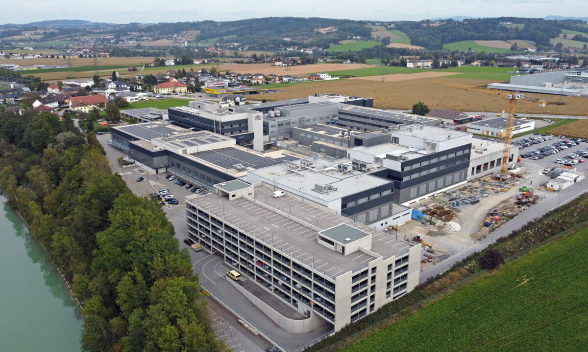
In parallel, our existing Manufacturing II building has been converted to offer nine new test rooms for the final assembly of EVG’s high-precision systems, as well as for technical source inspection of the systems by EVG’s customers. As a result, EVG’s headquarters today include a total of 62,000 m2 of plant area, including more than 8,100 m2 of production space, nearly 2,800 m2 of test room space, and more than 9,500 m2 of warehouse space. Manufacturing VI, EVG’s next phase of expansion provides for an additional 1,400 m2 of production and an equal amount of warehouse space, and is already under construction, with completion scheduled for the second half of this year (Feature image). Beyond that, initial plans are underway for further expansion of our manufacturing and cleanroom capacity on the near horizon.

Besides our production capacity expansion efforts, EVG has also significantly expanded its process development services. We launched our NILPhotonics® Competence Center and Heterogeneous Integration Competence Center™ (HICC) to serve as innovation incubators for our customers and partners, and shorten development cycles and time to market on new products and applications driven by advances in nanoimprint lithography, and system integration/packaging, respectively.
Our main goal with these centers of excellence is to provide flexibility and speed of process integration while ensuring the highest level of IP protection for every aspect of development. We work with customers and partners, ranging from start-ups to the world’s largest manufacturers and research institutes to jointly develop processes with EVG at our headquarters in Austria as well as in our cleanrooms in North America and Asia. Our cleanrooms are outfitted with our most advanced process tools and are designed to meet even the most stringent customer requirements, even allowing for virtual line concepts where wafers are reintroduced into customer fabs for further processing.
While adding new facilities and services is essential to EVG’s growth, the most important ingredient to our success as a global semiconductor equipment company is our people. This year, we achieved a new milestone with our global headcount surpassing 1,300 employees from 29 countries. Since our people are our most valued asset, it is critical that we invest in the well-being of our employees. A case in point, family friendliness has always been a top priority at EVG, and this year marks the 10th anniversary of “EVG Minis”, our in-house kindergarten and nursery, which provides free daycare to our employees. The EVG Minis started with eight children when we launched the program in 2013. Today, more than 60 children are looked after in two kindergartens and two toddler groups by a total of seven primary school teachers and five pedagogical assistants. We have already begun further extensions of the EVG Minis building as part of our ongoing construction projects.
EVG also firmly believes that it has a corporate responsibility to support a clean and sustainable environment. In recent years, we have implemented numerous energy-saving measures as well as expanded green energy production on-site. Currently, we have more than 4,850 m2 of roof area covered with photovoltaic panels, producing approximately 1.5 MW of power, with further expansions planned. Since 2020, the percentage of energy produced onsite with solar power versus our total energy production has increased by more than 4X. At the same time, the number of electric cars in our company fleet has increased by nearly 6X. In addition, our carbon efficiency ratio (the percentage of CO2-neutral and renewable energy versus total energy consumption is nearly 75 percent. These are just some of the numerous green initiatives EVG is implementing to reduce its carbon footprint. We recognize the need to address climate change and we are committed to playing our part.
It is truly an exciting time for EVG. 3D and heterogeneous integration have brought fusion and hybrid bonding front and center as critical processes for continuing PPAC scaling. This has fueled tremendous growth within EVG, enabling us to continue to invest in our technology, infrastructure, and people, which in turn helps us to continue to invest in our customers’ success. 2024 will be an amazing year for semiconductor innovation, with further advances in device architectures and packaging integration schemes such as backside power delivery, complementary FET, and 2D materials. Underpinning all these advances is wafer bonding, and as the market and technology leader in wafer bonding, EVG will be by our customers’ side as they march forward on their roadmaps with smaller, faster, more power-efficient, and lower cost-of-ownership products.
This article first appeared in the 2024 3D InCites Yearbook. Read the full issue here.