

The February issue of Chip Scale Review contained an interesting article entitled “Heterogeneous Chiplet Integration to Make Megachips” authored by members of the advanced technology division of MIT’s Lincoln Labs.
The work had previously been shown at the 2023 IEEE ECTC. While I don’t see anything revolutionary about their technology or the processes they are using, it does purport to broaden the use of chiplets, so let’s take a look at what they had to say…
Lincoln Labs authors noted that power consumption, always of interest, for extremely large area ICs (ELAICs) architecture is reduced. This is to be expected since, for example, in high-performance computing (HPC applications) power consumption comes primarily from moving data between chips rather than from on-chip computing operations. This “ELAIC architecture” reduces data movement by having chiplets with minimum chip-to-chip separation thereby reducing the loading of these I/O paths by at least an order of magnitude.
This article discusses a heterogeneous chip tiling technique that enables the realization of ELAICs that they claim could contain hundreds of closely spaced chiplets that are interconnected using RDL fabricated via lithographic processing. The ELAIC platform allows the tiling of known good chiplets (KGCs to make systems with close to the performance of a single chip monolithic device.
With this approach, the authors claim one can fabricate a large format “single-chip-like” SoC from advanced node KGD chiplets, thus increasing yield and performance.
The ELAIC structure, having 5-20um chip-to-chip spacing creates short ( i.e. 50-500um) electrical links for high bandwidth, low latency communications.
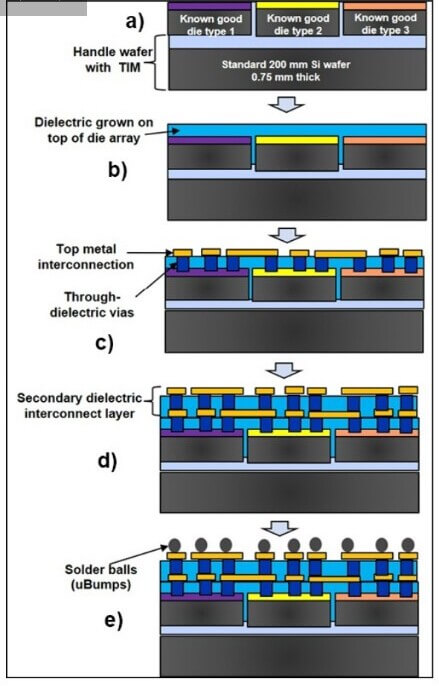
Lincoln Labs first developed an assembly process for maintaining narrow gaps between the chips and maintaining top chip surface planarity to allow thin dielectric deposition to make the RDL connections. They assembled various configurations using 5 x 5mm to 20 x 20mm chiplets to test chip surface planarity and chip spacing capabilities. There is little detail on this assembly process. If anything special is needed, it is not being reported. It is noted that an”… appropriate cleaning to remove dicing debris and give a smooth chip edge with minimal chipping” is reportedly critical for minimizing the chip-to-chip spacing.
The ELAIC process flow is shown in Figure 1. The RDL typically has multiple metal layers each separated by PECVD SiO2, PI, or BCB dielectric layers and connected using micro vias.
No discussion was included about the communication protocols that were / would have to be used to get the heterogeneous chiplets, possibly fabricated by different processes in different fabs, to be able to communicate with each other (i.e AIB vs UCIe ect). Seems like this would have a significant impact on the overall architecture of these multichip modules (MCMs) or systems-in-package (SiP).
Is the CHIPS Act Enough?
In a recent EE Times article by Nicholas Brathwaite, Founding Managing Partner, Celesta Capital, the question was asked: “Chips Are a National Security Issue: Is the CHIPS Act Enough?”. Brathwaite pointed out that currently, Taiwan produces about 60% of the world’s chips and 90% of the most advanced semiconductors.
He quickly answered his own question stating that “.. to truly eliminate potential geopolitical risks and regain the level of chip dominance it once had, the U.S. must do more.”

The article continued indicating that while the CHIPS legislation is a good start, three key factors will dictate the ability for countries to have true technological independence in the global chips war: R&D investment, availability of skilled labor, and sustainability.
R&D Investment
The CHIPS Act earmarked $13 billion to create two new entities dedicated to chip R&D: the National Semiconductor Technology Center (NSTC) and the National Advanced Packaging Manufacturing Program (NAPMP). These organizations can play a crucial role in pre-commercial research. But, asks Braithwaite, “ What will happen once this one-off legislation funding is gone? He concludes, and IFTLE concurs, that incorporating such funding into the larger federal R&D budget is essential.
IFTLE is also a supporter of a balanced budget and could offer the Govt many areas they could cut to continue support of this very important undertaking.
Skilled Labor
Braithwaite points out that the U.S. semiconductor industry is on track to face a shortfall of 300,000 engineers and 90,000 skilled technicians by 2030.
He proposes that a rapid way to help close this gap is to establish and expand chip-related training programs, including factory automation, chemical engineering, material science and advanced vacuum systems at technical colleges located near planned manufacturing centers. Addressing the labor gap in more advanced engineering and design roles will also require a concerted effort to grow the pipeline of U.S. STEM students, attract more of them to the semiconductor industry, and bring more STEM professionals into the U.S. economy from overseas.
Sustainability
Making chip production itself less environmentally intensive will require new approaches for powering production facilities, better monitoring and controlling of production processes, and recycling waste.
Braithwaite concludes with “To achieve its bold ambitions, the U.S. must develop a plan that solves for the entire end-to-end ecosystem – a network of hardware and software companies spanning design, materials, manufacturing and distribution. This will be a long-term, multifaceted undertaking”
For all the latest in advanced packaging technology stay linked to IFTLE…………….


