
The Department of Commerce (DoC) has announced Intel as the fourth program it will fund under the CHIPS and Science Act
CHIPS for America includes the CHIPS Program Office (responsible for manufacturing incentives), and the CHIPS Research and Development Office, (responsible for R&D programs). Both activities sit within the National Institute of Standards and Technology (NIST) at the Department of Commerce.
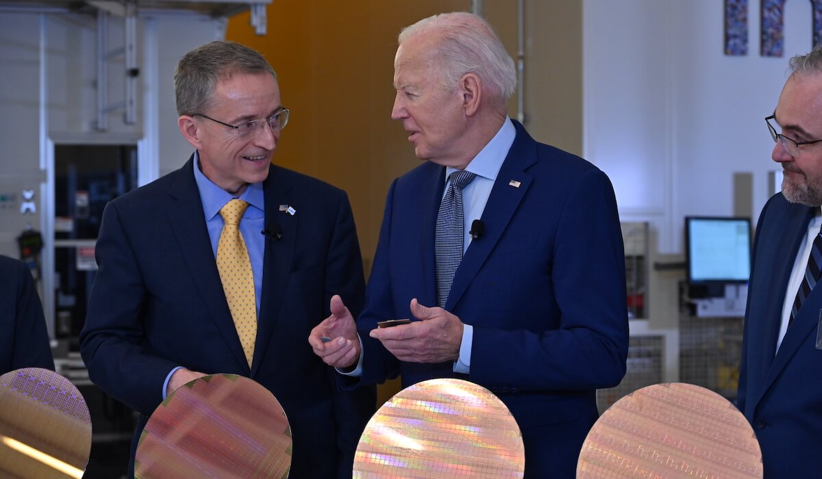
The DoC and Intel Corporation have reached a “preliminary memorandum of terms” to provide up to $8.5 billion in direct funding under the CHIPS and Science Act to “…strengthen the U.S. supply chain and re-establish American leadership in semiconductor manufacturing”. The award amounts are subject to due diligence and negotiation of a long-form term sheet and award documents are conditional on the achievement of certain milestones and remain subject to availability of funds.
The agreement also includes approximately $50 million in dedicated funding to develop the company’s semiconductor and construction workforce. This builds upon Intel’s workforce investments, totaling over $250 million in the past five years.
Intel expects its investments in the United States, over the next five years, to exceed $100 billion, as it expands capacity and capabilities in Arizona, New Mexico, Ohio, and Oregon.
The proposed CHIPS funding would include proposed investments in:
- Chandler, Arizona: Construction of two new leading-edge logic fabs and modernization of one existing fab, significantly increasing leading-edge logic capacity, including high volume domestic production of Intel 18A – the company’s most advanced chip design that reportedly enables higher performing, leading-edge chips through RibbonFET gate-all-around transistors and PowerVia backside power delivery.
- Rio Rancho, New Mexico: Modernization of two fabs into advanced packaging facilities to close an important gap in the domestic semiconductor supply chain. When in full production, this facility will be the largest advanced packaging facility in the United States.
- New Albany, Ohio: Creation of a new regional chipmaking ecosystem, anchored by the construction of two leading-edge logic fabs, expanded leading-edge foundry capacity, and supply chain diversification.
- Hillsboro, Oregon: Investment through the expansion and modernization of technology development facilities that will utilize the world’s first High NA EUV lithography equipment.
In addition to the direct funding of up to $8.5 billion, CHIPS will make up to $11 billion in loans to Intel. The company has indicated that it plans to claim the Department of the Treasury’s Investment Tax Credit, which is expected to be up to 25% of qualified capital expenditures.
RTX / AMD to Develop Next-gen Multi-Chip Package
Raytheon, has been awarded a $20MM contract through the Strategic and Spectrum Missions Advanced Resilient Trusted Systems (S2MARTS) consortium to develop a next-generation multi-chip package for use in ground, maritime, and airborne sensors.

Under the contract, Raytheon will package state-of-the-art commercial devices from industry partners like AMD to create a compact microelectronics package that will convert radio frequency energy to digital information with more bandwidth and higher data rates. The integration will result in new system capabilities designed with higher performance, lower power consumption and reduced weight.
“By teaming with commercial industry, we can incorporate cutting-edge technology into Department of Defense applications on a much faster timescale,” said Colin Whelan, president of Advanced Technology at Raytheon. “Together, we will deliver the first multi-chip package that features the latest in interconnect ability – which will provide new system capabilities to our warfighters.”
This multi-chip package will reportedly be created with the latest in industry-standard die-level interconnect ability, said to enable individual chiplets to reach their peak performance and achieve new system capabilities in a cost-effective and high-performance way. It’s designed for compatibility with Raytheon’s scalable sensor processing requirements.
Chiplets from commercial partners will be integrated onto a Raytheon-designed and fabricated interposer using the company’s 3D Universal Packaging (3DUP™) domestic silicon manufacturing process in Lompoc, California. This award will be managed by the National Security Technology Accelerator and administered by the Naval Surface Warfare Center Crane Division in Indiana.
For all the latest in Advanced Packaging stay linked to IFTLE………………

