
 If you have been following the announcements from Bob Patti and his company, NHanced Semiconductors, it would not be surprising if you were a bit confused about how all these announcements will be coming together. I know IFTLE was, so we approached longtime friend Bob Patti and came up with the following information.
NHanced ultimate goal is to supply both the commercial and military/aerospace markets. Aerospace and Defense currently account for 2/3 of its business. NHanced’s technical capabilities include:
Advanced Packaging:
- HDI edge packaging
- Chiplet integration
- TSV Insertion
- Covalent oxide bonding
- Hybrid copper and nickel bonding
- “True” heterogeneous integration
- Transfer print assembly
- Wafer reconstitution
- Die-to-die, die-to-wafer, and wafer-to-wafer 2.5D and 3D integration
Specialized Materials:
- Interposers: Silicon, glass, and fused silica
- Optical and electrical interconnect
- Advanced substrates: Silicon, GaN, GaAs, InP, GaSb, LINbO3, SiC, etc.
AP Assembly:
- Flip chip
- Solder ball drop
- Co-packaged optics
- Interposer and substrate
NHanced Expansion Plans – Location by Location
Batavia IL
NHanced Semiconductor’s headquarters is also its original site for design and test. Its capabilities are described as “complete front end and back end capability down to 12nm”. This site is reportedly supporting AI and HPC system developments.
Morrisville NC
NHanced’s current R&D and prototyping fab, just outside Research Triangle Park (RTP), was the original Ziptronix site where Ziptronix developed DBI and ZiBond or what is today called hybrid bonding.
The 25,000-square-foot facility includes a 7,000-square-foot clean space (class 100). Patti described the fab’s toolset as “…ideal for rapid prototyping with a focus on 3D-ICs and interposer assemblies.”
- In-house 2.5D/3D technology development
- In-house 2.5D/3D IC prototyping
- 100mm, 150mm, and 200mm wafer processing
- Fab processes include photo, etch, thin film deposition, surface prep, metallization, bonding, wafer thinning, CMP, pick-and-place
- Wafer-to-wafer, chip-to-wafer, and chiplet-to-interposer bonding
- Hybrid bonding
Morrisville is currently backlogged due to a lack of staff and equipment. Plans are to double the size of the Morrisville facility by acquiring the adjacent building.
Bloomington, IN
NHanced is currently bringing up a second site in Bloomington IN (home of Indiana University), which will include a 55K sq. ft. cleanroom and be capable of handling 75 – 200mm wafers. The company expects the first production wafers a year from now with an expected facility capacity of 5000 wafers/month. The Bloomington facility will be capable of many advanced packaging processes and will be a backup site for silicon/glass interposer fabrication. This facility will be semi-automated.
Odon, Indiana
The new advanced packaging facility (also known as the Westgate facility) is expected to be operational by the end of this year. This will be a fully automated facility with a focus on manufacturing silicon and glass interposers. The production goal for this facility is 100K interposers/month.
The future Odon site will be an “Interposer only” production site with the following attributes:
- Silicon and glass substrate interposers
- Up to 8 layers Cu damascene interconnect
- Down to 1um line/space
- 1-10um interconnect thickness
- TSVs: 50x300um, 25x200um, and 10x100um
- Hermetic hybrid bonded die and lids
- Full prototyping and low-volume assembly on site
Technologies at NHanced Semiconductors
Hybrid bonding
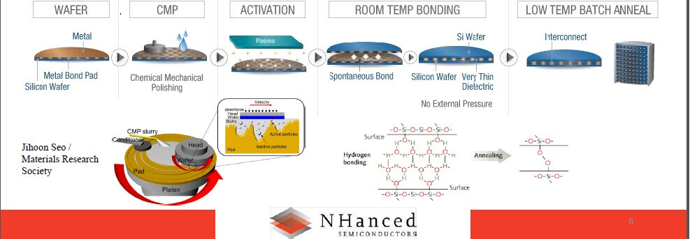
NHanced is one of the few development houses in the US that can deliver devices built with hybrid bonding technology (direct Cu-Cu bonding). As noted, its Morrisville facility is the original site where Ziptronix developed these technologies in the early 2000s.

NHanced was an early licensee of the technology and currently has many of the original Ziptronix staff currently employed at its Morrisville facility. They typically run the process with a 5-10um pitch (although the process is capable of going sub-micron). Surfaces are CMP’d down to 0.3nm RMS. Once bonded, annealing is typically done at 350 C° (Figure 1).
Interposer Technology
NHanced reports booming demand for interposers. They report 15 interposer programs underway today with another dozen in negotiation.
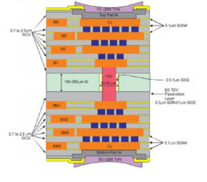
NHanced is developing both silicon and glass interposer technology. NHanced describes its interposer technology as being capable of 8 layers or interconnects as shown in figure 1.
NHanced Interposer capabilities include:
- Wafer size: 200mm
- Substrates: Silicon, borosilicate glass, fused silica (In development: post-fab formable metal interposers with ultra-low CTE)
- Pad finishes: Ni UBM, lead and no-lead bumps, ENIG, copper pillar, others
- TSV type: via first, copper fill, with aspect ratio up to 10:1
- TSV sizes: 50 x 400µm, 25 x 200µm, 10 x 100µm, or custom sizes
- TSV minimum pitch: 3X TSV diameter
- Interconnect layers (front- and back side): planarized damascene copper
- Interconnect layer design rules: 2µm line, 2µm space baseline, 1µm and 10µm options
- # of front-side layers: 4 baseline, options from 1-5 layers
- # of backside layers: 1 baseline, options from 1-5 layers
- Thick copper interconnect: 2µm baseline, options from 1µm to 10µm
- Reticle size: 44 x 22mm; with field stitching, more than 60 X 60mm
- Interposer Size – Up to full wafer
- Cadence process design kit (PDK)
In addition, NHanced is involved with several other advanced packaging technologies/application areas in addition to hybrid bonding and interposers including:
- Quilt packaging (Indiana IC)
- The HRL MECA process
- Microfluidics
- Photonics
- RAD Hard
- Quantum devices
- Memory
- Chiplet modules
- Advanced substrates: silicon, GaN, GaAs, InP, GaSb, LiNbO3, SiC, etc.
- Transfer printing
For all the latest in Advanced Packaging stay linked to IFTLE………………..


