


The university setting offers a valuable environment for future engineers to explore and learn about technologies that will become part of their daily lives when transitioning from school to a career. At the same time, universities working on microelectronics and advanced R&D are increasingly looking for more advanced manufacturing equipment that offers both reasonable upfront investment costs, and a low cost of ownership.
Over the next five years, we will see significant changes in the kinds of microelectronics projects and programs universities pursue. University fabs are moving toward advanced fab-level wafer processing and away from the benchtop beakers and wet benches not equipped to deal with new and emerging challenges. With the passage of the U.S. CHIPS and Science Act, universities are looking to take a major leap forward in the capability to transfer technology more readily to the chip manufacturing industry.
Engaging with advanced tools is also more interesting than working with wet benches, which will inspire students to join the industry and be better prepared to work in real fabs. This will be vital to filling the semiconductor industry’s need for skilled workers. According to a recent Semiconductor Industry Association (SIA) report, the workforce will grow to approximately 460,000 jobs by 2030, representing 33% growth from today’s 345,000 jobs. However, at the current degree completion rate, 58% of these projected new jobs (and 80% of projected new technical jobs) may go unfilled.
Universities are thus under added pressure to attract and excite students to enter the industry by providing relevant curriculums and imparting real-world skills. Bringing more advanced tools to universities will also mirror what’s being used in the semiconductor industry – essentially setting up universities to become an adjunct for industry development.
Some university cleanrooms are already adding the kinds of production-proven, fully automated high-volume tools found in today’s semiconductor facilities. While this level of investment is aspirational, other schools plan to spend significant funds on their cleanroom setups. They need affordable yet powerful tools to help them move toward industry-level offerings that allow them to optimize premium fab space.
Enabling the Lab-to-Fab Transition
Many universities looking to offer more leading-edge capabilities focus on advanced packaging (AP). According to market research firm Yole Group, this industry’s market value is projected to grow from US$ 44.3 billion in 2022 to US$ 78 billion by 2028 – a 10% CAGR. AI and machine learning enable data centers, automotive, 5G, and other applications that require powerful processors to handle the sheer volume of generated data. In turn, these devices necessitate the use of AP techniques.
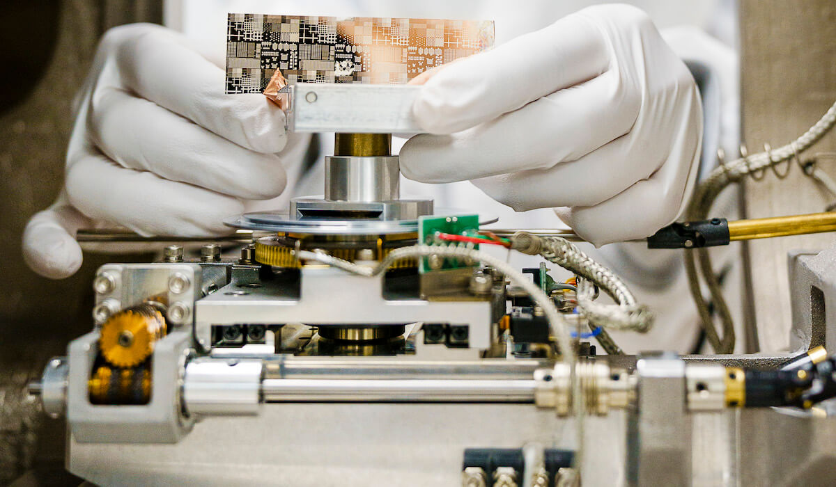
Electroplating is an essential AP process, enabling fast, cost-effective formation of electrical features and metallic connections. In addition, electroplating creates a huge opportunity for single-wafer processing systems. Universities are researching technologies such as ultra-high-aspect-ratio through-silicon via (TSV) features on semiconductor wafers and new areas like quantum computing, which uses novel processes and unique materials, such as indium and aluminum. Single-wafer systems can better accommodate these advanced processes and technologies than wet benches.

Leveraging TDC Expertise
ClassOne has worked with research institutes in Europe, such as Germany’s Fraunhofer ENAS Ferdinand-Braun-Institut, and VTT Technical Research Centre of Finland, as well as 3IT at Université de Sherbrooke in Canada. The company has also established relationships with several leading U.S. universities, including Georgia Institute of Technology, which is at the forefront of addressing the nation’s need for semiconductors.
A key aspect of this is the collaborative development efforts pursued in ClassOne’s Technology Development Center (TDC), where company engineers process customer wafers, develop and execute process experiments, and devise new products and enhancements to established tools. Customers can take advantage of technical training and demonstrations, while ClassOne expands its depth of knowledge via projects being pursued by universities, institutions, and corporate customers.
In conclusion, the semiconductor industry stands at a crucial juncture, marked by unprecedented demand for its products and an acute shortage of skilled professionals. The need for semiconductor firms to actively engage in programs that entice college students to join the industry cannot be overstated. The future of technology, from AI and autonomous vehicles to renewable energy solutions and healthcare advancements, depends on a robust and innovative semiconductor sector.
This article first appeared in the 2023 3D InCites Yearbook. Read the issue here.


