
We all knew it was coming….it was just a matter of time until it was announced. The Department of Commerce unveiled its 5th program under the CHIPS and Science Act, this time with TSMC, or more accurately TSMC Arizona Corporation (TSMC-AZ), a subsidiary of Taiwan Semiconductor Manufacturing Company Limited.
The DoC signed a non-binding preliminary memorandum of terms (PMT) to provide up to $6.6B in direct funding under the CHIPS and Science Act. TSMC will reportedly invest more than $65B for three leading-edge fabs in Phoenix AZ.
[Signing of the PMT triggers a comprehensive due diligence process on the proposed projects and continues negotiating or refining certain terms with the applicant. The final award terms may differ from the terms of the PMT being announced now.]
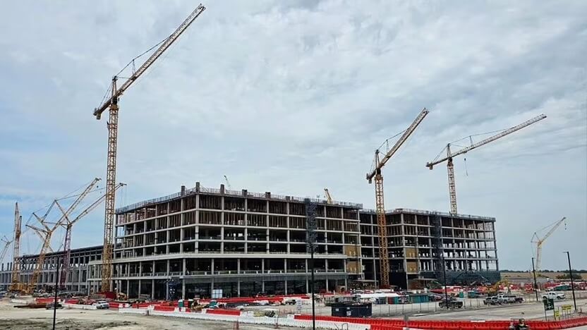
In addition, TSMC-AZ is committing to build an additional third fab before the end of the decade. TSMC’s three fabs are expected to bring the most advanced process node technologies to the U.S. The first fab will use 4nm FinFET process technologies, the second fab will use 2nm nanosheet process technology and the third fab will use 2nm or more advanced process technologies depending on customer demand. At full capacity, these three fabs will reportedly manufacture tens of millions of leading-edge chips. TSMC-AZ expects to begin high-volume production in the first fab in the U.S. by the first half of 2025. The second fab in Arizona is expected to begin production in 2028.
TSMC-AZ’s investment in the US is triggering investment across the supply chain, including 14 direct suppliers that plan to construct or expand plants in Arizona or other parts of the U.S.
Through its AZ fabs, TSMC will seek to better support key customers, including AMD, Apple, Nvidia, and Qualcomm.
TSMC-AZ also committed to supporting the development of advanced packaging capabilities creating the opportunity for TSMC-AZ customers to be able to purchase advanced chips that are made entirely on U.S. soil.
The agreement also proposes $50 million in dedicated funding to develop the company’s semiconductor and construction workforce. As part of its commitment to developing local talent, TSMC Arizona established one of the first state-supported Registered Apprenticeship programs for semiconductor technicians, with support from the City of Phoenix. TSMC’s U.S.-based recruiting team is also actively working with university programs around the country such as Arizona State, U Arizona, and Purdue.
In addition to the proposed direct funding of up to $6.6 billion, the CHIPS Program Office are prepared to make $5B in proposed loans available to TSMC-AZ under the PMT. The company has also indicated that it is planning to claim the Department of the Treasury’s Investment Tax Credit, which is expected to be up to 25% of qualified capital expenditures.
For comparison, Intel will be receiving $8.5B in grants and up to $11 billion in loans, so its total is almost double that of TSMC’s. In terms of direct funding, Intel will receive $2B more than its rival TSMC.
Samsung’s CHIPS Fund Plans
The Austin American-Statesman reported that the CHIPS & Science Act will announce, next week, that it is awarding between $6 billion and $7 billion to Samsung to expand its chip output in Taylor TX (northeast of Austin – Feature photo above).
The subsidy will reportedly go toward the construction of four facilities in Taylor including a $17 billion chipmaking plant (previously announced in 2021), a second factory, an advanced packaging facility, and a research and development center. It will also include an investment in another undisclosed location, which will more than double its U.S. investment to $44B.
In addition, during the first 10 years of the project, Samsung is expected to receive about $680 million in total tax breaks and other incentives from Taylor, Williamson County, the Taylor school district and the state.

The 6 million-square-foot plant sits on more than 1,200 acres. Initial production is currently expected in 2025.
More detail on this Samsung project is expected with the official announcement next week.
IMAPS & IPC to Host Onshoring Workshop
The International Microelectronics Assembly and Packaging Society (IMAPS) will host its 3rd annual workshop to discuss ongoing progress and forward-looking strategies to drive Onshoring Advanced Packaging and Assembly, April 29 – May 1, 2024, in Arlington, Virginia.
This workshop will bring Government agencies, the DIB (Defense Industrial Base) and Advanced Packaging and Assembly providers (OSATS) together to discuss their ongoing efforts to bring advanced packaging onshore.
This event’s mission is to engage the domestic semiconductor industry by providing progress updates on US Government and Defense initiatives that are critical to the onshoring of the microelectronic assembly and packaging supply chain. Additionally, emerging advanced packaging initiatives that are being driven by numerous Government agencies, including the Department of Commerce/NIST, DoD (SHIP/IBAS/Title III), and DARPA will be highlighted.
The workshop will feature highly informative keynote presentations, a comprehensive assortment of Technical and Work Force Development topical sessions with participation of invited speakers, panel discussions as well as a variety of networking opportunities. Attendance is for US citizens only………….
Keynotes include:
- Adele Ratcliff, Director of Innovation Capability and Modernization (ICAM) Office
- Dev Palmer, Next-Generation Microelectronics Manufacturing (NGMM) Program Managing Director, DARPA
- Dev Shenoy, Office of the Undersecretary of Defense, Director of the Defense Microelectronics Cross Functional Team
- Eric Lin, Deputy Director, CHIPS Research and Development Program
- George Orji, National Advanced Packaging Manufacturing Program (NAPMP)
- Joshua T. Hawke, Ph.D., Navy – OUSD R&E RF/OE Initiatives, Technical Execution Area Lead
- Jay Lewis, Director, National Semiconductor Technology Center (NSTC) Program
For all the latest in Advanced Packaging stay linked to IFTLE……………………………………


